Dear customer, welcome to MINKINZI-China leading manufacturer for flex circuit, rigid flex circuit, rigid PCB and PCBA. Especially Difficult Projects. .
Dear customer, welcome to MINKINZI-China leading manufacturer for flex circuit, rigid flex circuit, rigid PCB and PCBA. Especially Difficult Projects. .
Layers:64
Material:FR4 Tg180
Board Thickness:6.89mm
Min Blind/Buried hole size:0.2mm(8mil)
Surface treatment: ENIG
Impedance Control:single ended 50,
differential 110Ω+/-10%
Description :
Impedance is the combination of the capacitance and inductance of a circuit when operated at high frequency. Though also measured in Ohms, it is somewhat different than resistance which is a DC characteristic. Impedance is an AC characteristic, meaning that it is related to frequency, resistance is not.
Controlled impedance should be used, when a signal must have a particular impedance in order to function properly. In high frequency applications matching the impedance of PCB traces is important in maintaining data integrity and signal clarity. If the impedance of the PCB trace connecting two components does not match the components' characteristic impedance, there may be increased switching times within the device or the circuit. There may also be random errors.
Impedance Control PCB are used in Telecommunications, Computing 100MHz and above, High Quality Analog Video, Signal Processing, RF Communication, etc.
Applications :

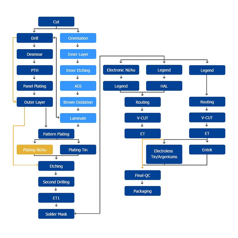
Flow Chart :

Capability :
| Layers | 1-136 | |
| Technology | Blind and Buried Via, HDI,Hollow out, Selective Hard gold plating,Depth Control,Press fit hole, Edge Half-plated hole, Back drill, Countersink hole, Plated edge, Peelable solder mask, Imedance control, Gold Finger, Fill via with resin and other technology. | |
| Materials | Standard FR4/Mid-Tg FR4/Hi-Tg FR4,CEM-1/CEM 3,PTFE,Rogers,Arlon,Taconic, Teflon,Isola,ITEQ,Dupont,Polyimide,Metal Core Material,Ventec,Nelco | |
| Max. PCB Panel Size | 9000mmx820mm | |
| Board Thickness | 0.2-12mm | |
| Board Thickness Tolerance | ±10% | |
| Copper thickness | 0.5 OZ to 22 OZ | |
| copper thickness in hole | copper thickness in hole: >25.0 um(>1mil) | |
| Min Conductor Line Trace/Space | Inner Layers:≧3/3mil(0.075/0.075mm for 1/2oz base Copper) | |
| Outer Layers:≧3.5/3.5mil | ||
| For Via in Pad | Resin plugged hole size | 0.3-0.75mm |
| Resin plugged board thickness | 0.3-8mm | |
| Resin plugged maximum aspect ratio | 40:1 | |
| Resin plugged minimum hole to hole space(mm) | 0.65mm | |
| For HDI | Min. mechanical drilling hole diameter | 0.15mm |
| Min. laser drilling hole diameter | 0.075mm | |
| Max. aspect(micro-via) | 1:1 | |
| Max. dielectric thickness for laser drill | 0.05-0.15mm | |
| Bottom pad size(under micro-via) | Hole Size+0.17mm | |
| Top side pad size(on micro-via) | Hole Size+0.15mm | |
| Copper filling | Y | |
| Via in pad design | Y | |
| Buried hole resin plugged | Y | |
| Min. via size can be copper filled | 0.075mm | |
| Min plated hole size | 20um(0.8mil) | |
| Min Blind/Buried hole size | 0.2mm(8mil) | |
| Min Annular Ring | ±0.076mm(±3mil) | |
| Min width of cutout (NPTH) | 0.8mm | |
| Min width of slot hole (PTH) | 0.6mm | |
| Solder mask color | green, red, blue, white, yellow, purple, black, orange, LPI, matt green,matt black | |
| Silkscreen color | White, Yellow, Red, Black | |
| Surface finish | ENIG, ENEPIG,Immersion Tin, HASL, HASL-LF, OSP,Selective OSP, Gold finger, Immersion Silver,Bare Copper,Hard gold plating, Selective hard gold plating,Selective Immersion gold,Selective gold plating,HASL-LF+Selective Immersion gold,HASL-LF+Selective gold plating,HASL-LF+OSP,and other surface treatments. | |
| Outline | Routing, V-cut, Bridge, Stamp hole | |
| Outline Tolerance | ±0.15mm (±6mil) | |
| Hole Tolerance | PTH +/-3mil | |
| NPTH +/-2mil | ||
| Controled Impendence | +/-5%(<50Ω), +/-10%(≧50Ω) | |
| E-Test | Flying probe test:0.4-6.0mm, max 19.6"*23.5" | |
| Min spacing from test pad to board edge:0.5mm | ||
| Min conductive resistance:5Ω | ||
| Max insulation resistance:250mΩ | ||
| Max test voltage:500V | ||
| Min test pad diameter:6mil | ||
| Min test pad to pad spacing:10mil | ||
| Max test pad to pad spacing:10mil | ||
| Max test current:200MA | ||
| AOI | Orbotech SK-75 AOI:0.05-6.0mm, max23.5"*23.5" | |
| Orbotech Ves machine:0.05-6.0mm, max23.5"*23.5" | ||
| Profiling | Punching,Routing, V-CUT,Beveling | |

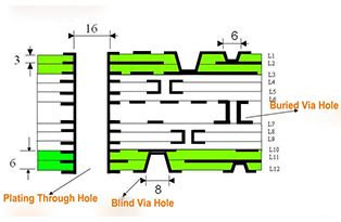
Difference of Blind Via Hole(BVHBuried Via Hole (BVH) and Plating Through Hole(PTH)
Connect the outermost circuit of the PCB and the adjacent inner layer with plated through-hole, since we cannot see the opposite, so it is called ...

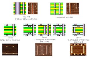
Benefits of HDI PCB Technology with Micro Circuits
Shorter PCB manufacturing lead times and improved device performance for Flip Chip, BGA, MCM, SIP technologies and medical devices. A...
Cell: +86 186 6584 1838 Telephone:+86 0769 3320 0710
Songshan Lake International Creativity Design Industry Park,No. 10, West Industrial Road,Songshan Lake High-Tech Dist.,Dongguan,China.523808.