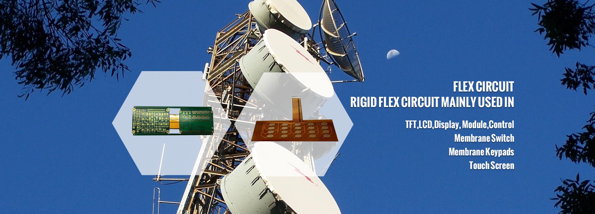
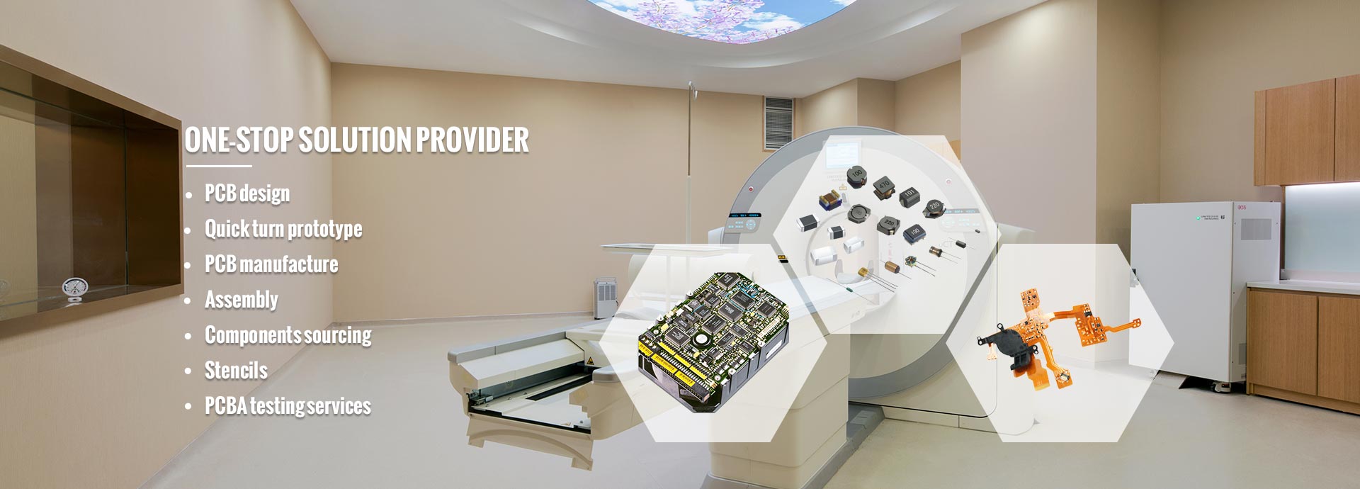
Dear Partners, welcome to MINKINZI – China’s Trusted End-to-End Manufacturing Partner, with 20 years of expertise, we specialize in: Design & Development → PCB Fabrication → PCBA Assembly → Box-Build Assembly. ODM/OEM/Contract Manufacturing tailored to global standards. Support DFM. .

  • Smartwatch|Fitness Tracker PCBA Design| Assembly – Fast Prototyping

  • Smartwatch|Fitness Tracker PCBA Design| Assembly – Fast Prototyping

  • Smartwatch|Fitness Tracker PCBA Design| Assembly – Fast Prototyping

  • Smartwatch|Fitness Tracker PCBA Design| Assembly – Fast Prototyping

  • Smartwatch|Fitness Tracker PCBA Design| Assembly – Fast Prototyping

  • Smartwatch|Fitness Tracker PCBA Design| Assembly – Fast Prototyping

Smartwatch|Fitness Tracker PCBA Design| Assembly – Fast Prototyping

  1. Bare pcb design/layout, Bare pcb manufacturing, Max 56 layer HDI

  2. Component sourcing from orginal IC factory from global warhouse, competitive price.

  3. Do SMT, Assembly, Functional test.

  4. Conformal Coating, yes.

  5. From bare pcb, pcba to final whole Smart wearable device.


Share

Description :

Smartwatch|Fitness Tracker PCBA Design| Assembly – Fast Prototyping

Smartwatch|Fitness Tracker PCBA Design| Assembly – Fast Prototyping

Advanced PCB & PCBA Solutions for Next-Gen Wearable Smart Devices | Expert Manufacturing

Powering Innovation in Wearable Technology: Flexible PCBs, Rigid PCBs, Rigid-Flex PCBs, and advanced PCBA are the foundational technologies enabling cutting-edge wearable smart devices. As demand surges for smarter, smaller, and more reliable wearables, partnering with a certified PCB manufacturer and full-service PCBA assembly partner with expertise in wearable electronics is critical. We deliver high-reliability, miniaturized solutions meeting stringent industry demands.

I. Critical PCB Technologies for Wearables (Focus: Capabilities & Benefits)

  1. High-Performance Flexible PCBs (FPC):

    • Robust Material: Polyimide (PI) substrate (-200°C to 426°C, Dk≈3.5).

    • Precision Circuits: Ultra-fine lines ≤50μm width/spacing (±7% impedance control).

    • Proven Durability: Passes rigorous 100k+ bend tests (R≥1mm).

    • Core Function: Enable dynamic bending (100,000+ cycles) and waterproofing (IP68+) for ultimate device reliability in motion.

    • Key Advantages & Specs:

    • Ideal For: Bands, straps, foldable sections, flexible sensors.

  2. Reliable Rigid PCBs:

    • Stable Foundation: High-Tg FR-4 material (Tg ≥170°C).

    • Complex Routing: Supports 4-12 layers, suitable for medium/low-speed signals (≥75μm line/space).

    • Core Function: Provide structural support and high-density wiring for core electronics (CPU, PMIC) ensuring signal integrity.

    • Key Advantages & Specs:

    • Ideal For: Main device bodies (e.g., smartwatch motherboards), controller hubs.

  3. Integrated Rigid-Flex PCBs:

    • Precision Bonding: Rigid-flex lamination tolerance ≤ ±2%.

    • Optimized Bending: Transition zones ≥5mm, bend radius ≥1.5x board thickness.

    • Core Function: Combine 3D design flexibility with rigid stabilityreducing connectors and boosting reliability by 30% in space-constrained devices.

    • Key Advantages & Specs:

    • Ideal For: AR/VR headsets, foldable phones, complex medical wearables.

II. Advanced PCBA: The Intelligence Hub of Wearables (Focus: Integration & Miniaturization)

  • Seamless Function Integration: Expertly assembles sensors (heart rate, SpO₂, accelerometer), wireless modules (Bluetooth 5.x, Wi-Fi), ultra-low-power MCUs, and battery management ICs.

  • Ultra-Miniaturization Expertise:

    • Micro Component Placement: High-yield mounting of 01005 packages (0.4x0.2mm, ±25μm accuracy).

    • Space-Saving Tech: Implements SiP (System-in-Package) to reduce PCB area by 30%.

  • Optimized Power Efficiency: Designs for ultra-low standby current (≤10μA)maximizing battery life – a critical user demand.

III. Key Wearable Applications We Enable (Focus: Solutions & Performance)

  • Health & Medical Monitoring:

    • Smart Watches: Medical-grade ECG, real-time HR/SpO₂ monitoring (≥100Hz sampling).

    • Diagnostic Patches: Accurate blood glucose monitoring (<5% error), FDA/CE compliant designs.

  • Sports & Fitness Tracking:

    • Activity Trackers: Precise GPS positioning, >90% accurate calorie calculation.

    • AR Glasses: Low-latency bone conduction audio (<50ms), real-time navigation.

  • Emerging Innovations:

    • Smart Textiles: Seamless integration of fabric-based temp/pressure sensors.

    • Haptic Feedback: Fast-response micro-vibration arrays (≤5ms) for realistic touch simulation.

IV. Our Certified Wearable Manufacturing Excellence (Focus: Trust & Capability)

  1. PCB Factory Capabilities:

    • Advanced Processes: RTR (Roll-to-Roll) FPC lines, laser drilling (±10μm), ≤50μm layer alignment.

    • Rigorous Reliability Testing: Thermal cycling (-40°C to +125°C, 1000x), THB (85°C/85%RH, 168h).

    • Global Certifications: ISO 9001, IATF 16949 (Automotive), IPC-6013 Class 3 (Flex/Rigid-Flex).

  2. PCBA Factory Expertise:

    • Precision Assembly: >99.95% yield on 0201 components, 100% 3D SPI inspection.

    • Gentle Soldering: Controlled lead-free reflow profiles (245±5°C peak) for FPC safety.

    • Comprehensive Testing: Full RF validation (BT 5.0/5.2, Wi-Fi), >98% FCT coverage.

  3. End-to-End Product Assembly:

    • Robust Design Validation: IP68 waterproofing (1m/30min), MIL-STD drop testing (1.5m/26x).

    • Biocompatible Materials: ISO 10993 certified skin-contact components.

    • Responsible Supply Chain: Full component traceability, strict RoHS/REACH compliance.

V. Partnering for the Future of Wearables (Focus: Innovation & Partnership)

  • Leading Material Science: Adopting LCP substrates for 5G/6G wearables, reducing high-frequency signal loss by 50% vs. PI.

  • Smart Manufacturing: AI-powered visual defect detection (>99% accuracy), Digital Factory integration (OEE ≥85%).

  • Agile Support: Low MOQ (≤100pcs) friendly, rapid prototyping (≤72 hours) to accelerate your time-to-market.


The Role of Advanced Circuit Technologies in Smart Wearable Devices: FPCs, PCBs, Rigid-Flex & PCBA

Smart wearable technology has evolved far beyond basic step counting—it now sits at the cutting edge of healthcare innovation, human-computer interaction, and seamless personal connectivity. Behind every breakthrough in wearables—from medical-grade biosensors to ultra-slim hearables—lies a critical enabler: advanced printed circuit board (PCB) technology. Specifically, Flexible Printed Circuits (FPCs), Rigid PCBs, Rigid-Flex PCBs, and fully assembled Printed Circuit Board Assemblies (PCBAs) are no longer just supporting components; they are strategic differentiators that define performance, reliability, comfort, and miniaturization in next-generation wearable devices.


1. Why Advanced PCB Technology Is Crucial for Wearable Electronics

Wearable devices operate under extreme constraints: limited space, constant motion, exposure to moisture and heat, and the need for all-day comfort. Traditional wiring or rigid interconnects simply can’t meet these demands. This is where advanced PCB solutions come into play—offering miniaturization, durability, signal integrity, and design flexibility that are indispensable in modern wearables.


2. Flexible Printed Circuits (FPCs): Enabling Lightweight, Conformable Designs

Core Value:
FPCs deliver exceptional flexibility and dynamic bendability, allowing them to conform seamlessly to curved body surfaces like wrists, ears, and joints. With typical thicknesses under 0.2 mm, they enable ultra-thin, lightweight designs critical for long-term user comfort.

Key Applications:

  • Interconnecting biosensors (heart rate, SpO₂, skin temperature) with main control units

  • Internal wiring in smartwatch bands, earbud stems, and foldable displays

  • Medical-grade patches for continuous ECG, EEG, or glucose monitoring

✅ Ideal for: Health monitors, hearables, implantable sensors, skin-contact diagnostic patches


3. Rigid PCBs: Delivering Stability and High-Speed Performance

Core Value:
Rigid PCBs provide the structural backbone of wearable electronics, hosting critical ICs such as microcontrollers (MCUs), Bluetooth Low Energy (BLE) modules, power management ICs (PMICs), RF transceivers, and memory chips. They ensure mechanical stabilitythermal resilience, and superior signal integrity—especially vital for high-speed digital circuits.

Typical Use Cases:

  • Main processor boards in smartwatches, AR/VR headsets, and fitness trackers

  • Power regulation systems requiring efficient heat dissipation

  • Impedance-controlled traces for RF and high-speed data transmission

✅ Best suited for: Centralized computing modules where processing power, thermal management, and electrical stability are paramount


4. Rigid-Flex PCBs: The Gold Standard for Space-Constrained Wearables

Core Value:
Rigid-flex PCBs merge the structural strength of rigid boards with the dynamic adaptability of flexible circuits, creating an integrated solution that eliminates connectors, reduces assembly complexity, and enables unprecedented miniaturization. This hybrid architecture is rapidly becoming the go-to choice for premium wearable devices.

Critical Advantages:

BenefitImpact on Wearable Design
Space savings (>30%)Enables slimmer profiles and ergonomic form factors
Shorter signal pathsReduces noise, signal loss, and EMI—critical for accurate biometric sensing
High flex durability (>100,000 cycles)Survives repeated motion in hinge zones (e.g., folding watches, rotating bands)
Fewer interconnectsLowers failure rates, improves reliability, simplifies assembly
Improved thermal and mechanical performanceDistributes stress and supports localized heat dissipation

Real-World Applications:

  • Hinge interconnects in Samsung Galaxy Watch foldable variants

  • Internal cabling in Apple AirPods Pro and other TWS earphones

  • Sensor arrays in Meta Quest VR headsets and Oura Ring-style smart rings

  • Implantable and patch-based medical devices requiring long-term reliability

✅ Perfect for: Premium consumer electronics, medical diagnostics, aerospace wearables, and any application demanding maximum reliability in minimal space

Rigid-flex PCBs not only reduce part count but also enhance overall system-level performance by minimizing impedance mismatches, reducing solder joint fatigue, and enabling true 3D packaging architectures.


5. PCBAs: From Bare Boards to Fully Functional Systems

A bare PCB—whether rigid, flex, or rigid-flex—is only half the story. The real value emerges in the PCBA (Printed Circuit Board Assembly) stage, where precision surface-mount technology (SMT), automated optical inspection (AOI), and rigorous testing turn circuits into intelligent, functional systems.

Why PCBA Quality Matters in Wearables:

  • Ensures reliable attachment of sub-1mm components (e.g., 01005 passives, WLCSP packages)

  • Enables conformal coating for sweat/moisture resistance

  • Supports reworkability and traceability for medical-grade compliance (ISO 13485, IEC 60601)

  • Facilitates integration with firmware, wireless protocols (BLE, Zigbee, NFC), and cloud connectivity

Top-tier contract manufacturers leverage ultra-fine pitch SMT lineshelium leak testing, and automated X-ray inspection (AXI) to ensure defect-free assemblies—even in densely packed wearable modules.


Emerging Trends Shaping the Future

Manufacturers investing in high-layer-count rigid-flex stacksHDI (High-Density Interconnect) designs, and impedance-controlled fabrication will lead the next wave of innovation.


Applications :

Smartwatch|Fitness Tracker PCBA Design| Assembly – Fast Prototyping

Powering Next-Gen Smart Wearables: The Critical Role of Advanced PCBAs & Specialized OEM Manufacturing

The explosive growth of the smart wearable market (watches, trackers, glasses, patches) demands unparalleled precision and reliability from its core electronics. Printed Circuit Boards (PCBs) and Printed Circuit Board Assemblies (PCBAs) are fundamental to achieving the slim designs, extended battery life, and robust functionality users demand. Partnering with a specialized PCBA OEM (Original Equipment Manufacturer) is no longer optional – it's a strategic imperative for success.

I. Why Advanced PCBs & PCBAs are Non-Negotiable for Wearable Devices

Miniaturization & High-Density Integration:

PCB: Requires Flexible PCBs (FPC) or Rigid-Flex PCBs to conform to ergonomic curves and fit within ultra-compact spaces.

PCBA: Achieves extreme miniaturization via high-precision SMT assembly, utilizing micro-components (e.g., 01005 chips). This is essential for meeting stringent lightweight and compact form factor requirements.

Ultra-Low Power & Enhanced Reliability:

PCB: Needs optimized layer stackups and impedance control to minimize power loss, crucial for sensitive signal transmission (e.g., heart rate monitoring, SpO2 sensors).

PCBA: Incorporates specially selected ultra-low-power chipsets (e.g., BLE modules) and employs protective conformal coatings for water resistance (IP ratings) and sweatproofing, ensuring stability during intense activity and outdoor use.

Multifunctional System-on-Board (SoB) Design:

PCBA: Integrates complex functionality onto a single board: sensors (accelerometer, gyro, bio-sensors), wireless connectivity (Bluetooth Low Energy, WiFi, GPS/GNSS), processing units, and power management. This enables sophisticated features like fitness tracking, health monitoring, and seamless smartphone connectivity.

II. The Undeniable Value of a Specialized Wearables PCBA OEM Partner

Choosing the right electronics manufacturing partner is critical. A professional PCBA OEM/subcontractor delivers tangible value beyond basic assembly:

Technical Expertise & Capability Assurance:

DFM (Design for Manufacturability): Early design optimization prevents costly flaws common in wearables (e.g., short circuits from inadequate component spacing).

Component Sourcing & Supply Chain Resilience: Access to stable, vetted supply chains mitigates risks of shortages and cost volatility for specialized components (e.g., low-power MCUs, sensors).

Advanced Process Control: Mastery of micro-pitch SMT (01005 components), precision soldering (selective, reflow), and flexible circuit assembly ensures high yields for complex, miniaturized designs.

Rigorous End-to-End Quality Control:

Environmental Stress Testing: Temperature/Humidity cycling (e.g., -20°C to +60°C) simulates real-world extremes.

Mechanical Stress Testing: Drop and vibration tests replicate impacts encountered during sports and daily activities.

Incoming Material Inspection: Screens PCB substrates for defects (microcracks, copper integrity) and verifies component authenticity/batch consistency.

In-Process Monitoring: Employs Automated Optical Inspection (AOI) and X-Ray Inspection to detect soldering defects (bridging, voids, BGA cold joints) instantly.

Comprehensive Reliability Testing:

Cost Efficiency & Speed-to-Market:

Scaled Procurement: Leverages buying power to reduce BOM costs for high-volume passives (resistors, capacitors).

Agile & Flexible Production: Supports rapid prototyping, low-volume builds, and high-volume scaling. Enables faster iterations (e.g., smart glasses prototypes) and dramatically shortens time-to-market.

III. Choosing the Right Wearables PCBA Partner: Essential Selection Criteria

When vetting potential OEM partners, prioritize these critical factors:

Technical Capability Fit:

✅ Proven experience with Flexible PCBs (FPC) and HDI PCBs?

✅ Does SMT line precision support ultra-fine pitch components (e.g., 0.3mm pitch BGA/CSP)?

Compliance & Quality Certifications:

✅ Hold relevant Quality Certifications (e.g., ISO 13485 for medical wearables, IATF 16949)?

✅ Does RF design/manufacturing comply with target market regulations (e.g., FCC, CE, RED, SRRC)?

Supply Chain Stability & Agility:

✅ Offers component alternates/second sources to mitigate supply chain disruption risks?

✅ Provides local warehousing/inventory management options to reduce logistics lead times?

Conclusion: Accelerate Your Wearable Success with Expert PCBA Partnership

The performance, reliability, and user experience of your smart wearable devices hinge on optimized PCBA design and flawless, precision manufacturing. Partnering with a specialized PCBA OEM unlocks critical advantages:

Guaranteed Miniaturization & Functionality: Achieve sleek designs packed with features.

Uncompromising Reliability: Ensure robust performance in demanding environments.

Predictable Quality & Compliance: Navigate regulations with confidence.

Optimized Costs & Faster Launch: Scale efficiently and beat competitors to market.

Ready to build superior smart wearables? Partner with a PCBA expert who understands your unique challenges.


Flow Chart :

1. Customer share their idea with us, we design pcb, select component, make schematic diagram,pick and place file, BOM, outer box design.

Smartwatch|Fitness Tracker PCBA Design| Assembly – Fast Prototyping

Smartwatch|Fitness Tracker PCBA Design| Assembly – Fast Prototyping

Smartwatch|Fitness Tracker PCBA Design| Assembly – Fast Prototyping

Smartwatch|Fitness Tracker PCBA Design| Assembly – Fast Prototyping

Smartwatch|Fitness Tracker PCBA Design| Assembly – Fast Prototyping

2. SMT, Assembly, Test

Smartwatch|Fitness Tracker PCBA Design| Assembly – Fast Prototyping

Smartwatch|Fitness Tracker PCBA Design| Assembly – Fast Prototyping

Smartwatch|Fitness Tracker PCBA Design| Assembly – Fast Prototyping

Smartwatch|Fitness Tracker PCBA Design| Assembly – Fast Prototyping

Smartwatch|Fitness Tracker PCBA Design| Assembly – Fast Prototyping


Smart Wearable Product Development to Mass Production: A Complete Guide [2025]

The global smart wearable market is projected to surpass $150 billion by 2027, driven by rising demand in healthcare, fitness, and AI-driven personalization. Successfully bringing a smart wearable from concept to mass production requires meticulous planning across hardware, software, design, compliance, and supply chain management.

This comprehensive guide outlines the end-to-end development lifecycle, key engineering decisions, risk mitigation strategies, and real-world case studies — empowering innovators, startups, and OEMs to accelerate time-to-market and achieve high-yield, scalable manufacturing.


I. End-to-End Smart Wearable Development Process

1. Solution Definition & Feasibility Assessment

Before any design begins, clearly define:

  • Target User Segment: Athletes, elderly monitoring, children’s safety, medical patients

  • Core Functional Requirements: Heart rate tracking, SpO₂ monitoring, GPS positioning, AI voice interaction, emergency alerts

Technical Evaluation Checklist:

  • Sensor selection: PPG (photoplethysmography) sensors for heart rate, 6-axis IMUs for motion detection

  • Wireless connectivity: Bluetooth Low Energy 5.3 (BLE) for low power; optional Wi-Fi/NFC/BDS (BeiDou)

  • Processor architecture: ARM Cortex-M series MCUs for real-time performance with ultra-low power consumption

 Real-World Example: Huawei Watch Ultimate integrates satellite-based emergency calling via BeiDou, solving critical communication gaps during outdoor adventures.
RingConn's smart ring leverages clinical-grade photonic sensors to deliver continuous health monitoring, achieving over 400,000 annual export units through precision biometrics.


2. Hardware Design & Component Selection

Choosing reliable components ensures long-term product stability and scalability.

ComponentRecommended Models / BrandsUse Case Examples
Main MCUNordic nRF5340, Dialog DA1469xXiaomi Mi Band: ultra-low-power BLE processing
Motion Sensor (IMU)Bosch BMI270 (6-axis accelerometer + gyroscope)Accurate step counting, fall detection
Optical SensorTexas Instruments AFE4490Medical-grade PPG data acquisition
BatteryEVE Energy Li-Po 300mAhEnables up to 7-day battery life
Display ModuleBOE 1.3" AMOLEDHigh-resolution visuals on premium wearables

PCB Design Best Practices

  • Use 4–32 layer PCBs with controlled impedance (±10%) for signal integrity

  • Implement ground shielding and differential routing for RF modules

  • Utilize Cadence Allegro or Altium Designer for EMI/EMC-compliant layout

  • Optimize trace lengths for high-speed interfaces like SPI and I²C


3. Embedded Software & Algorithm Development

A robust firmware stack enables accurate sensing, efficient power use, and seamless cloud integration.

RTOS & Firmware Stack

  • Operating System: FreeRTOS or RT-Thread for lightweight real-time control

  • Programming Language: C/C++ for driver-level access and memory optimization

  • Middleware: BLE stack (Nordic SoftDevice), sensor fusion library (Bosch Xensiv)

Key Algorithms

  • Step Counting: Adaptive filtering + peak detection algorithm to reduce false positives

  • Sleep Staging: Multimodal fusion using heart rate variability (HRV), body movement, and temperature

  • Activity Recognition: Machine learning models trained on accelerometer data (walking, running, sleeping)

Cloud & Data Sync

  • Protocol: MQTT over TLS 1.3 for secure, low-bandwidth transmission

  • Cloud Platforms: AWS IoT Core, Alibaba Cloud IoT, or Microsoft Azure IoT Hub

  • Features: Over-the-air (OTA) updates, remote diagnostics, user behavior analytics


4. Industrial Design & Ergonomics

Comfort, aesthetics, and durability are crucial for user adoption.

Material Choices

PartRecommended MaterialsBenefits
Housing6061 Aerospace Aluminum Alloy (premium), PC+ABS (cost-effective)Lightweight, strong, corrosion-resistant
StrapMedical-grade silicone, fluoroelastomerHypoallergenic, sweat-resistant
CoatingIP coating, nano-ceramic finishEnhanced scratch and UV resistance

Innovation Spotlight: Huawei’s Xuanji Sensing System uses biomechanical modeling to optimize curvature and weight distribution, improving wearing comfort by 38% based on ergonomic testing.


5. Manufacturing & Quality Assurance

Scalable production demands strict process control and automated validation.

SMT Assembly Line Setup

  • Stencil thickness: 0.1 mm for fine-pitch components

  • Solder paste: SAC305 lead-free alloy (RoHS compliant)

  • Reflow profile: Nitrogen-assisted reflow to reduce oxidation

  • AOI (Automated Optical Inspection): Defect detection rate < 500 ppm

Final Assembly Steps

  1. Laser welding of coin-cell battery

  2. FPC (flexible printed circuit) connection between display and mainboard

  3. Encapsulation with waterproof adhesive (IP68 rated)

  4. Barometric pressure test for water resistance verification

Critical Test Procedures

Test TypeStandardEquipment Used
Functional TestingHeart rate accuracy ±2 bpmSimulated human pulse generator
Environmental ReliabilityOperation at -10°C to +40°C for 8 hrsThermal chamber
RF PerformanceStable BLE connection within 10 metersWireless comprehensive tester (e.g., Anritsu MT8852B)
Drop & Vibration TestMIL-STD-810G complianceMechanical shaker table

6. Mass Production Control & Yield Management

Achieving commercial success depends on consistent quality and traceability.

KPI Targets for High-Volume Production

  • First Pass Yield (FPY): > 95%

  • Mean Time Between Failures (MTBF): ≥ 100,000 hours (~11.4 years)

  • Traceability: Unique SN code per unit linked to material batch, production line, and test logs

✅ Best Practice: Deploy MES (Manufacturing Execution System) for real-time monitoring of yield trends, defect root cause analysis, and predictive maintenance.


II. Critical Success Factors & Risk Mitigation

1. Power Consumption Optimization

Battery life directly impacts user satisfaction.

Strategies:

  • Dynamic Voltage Scaling (DVS): Adjust CPU frequency/voltage based on workload

  • Event-Driven Wake-Up: Use low-power accelerometers (e.g., ADI ADXL367) to wake system only when motion detected

  • Display Duty Cycling: Turn off OLED after 5 seconds of inactivity

  • BLE Advertising Interval Tuning: Balance responsiveness and power savings


2. Data Privacy & Security Compliance

Wearables handle sensitive biometric data — security must be built-in.

Security Layers

  • Hardware Encryption: Secure element chips (e.g., Infineon OPTIGA™ TPM)

  • Secure Boot & OTA Signing: Prevent unauthorized firmware flashing

  • Transport Layer Security: Enforce TLS 1.3 for all cloud communications

  • Local Data Protection: AES-256 encryption for stored health records

Non-compliance risks include regulatory penalties and loss of consumer trust — especially in EU (GDPR) and US (HIPAA-related applications).


3. Regulatory Certification Pathways

Meeting regional standards is mandatory before market entry.

CertificationApplicable RegionsRequirements
FCC Part 15BUSAElectromagnetic interference (EMI) limits
CE MarkingEuropeEMC, LVD, RED directives
FDA 510(k) / CE Class I/IIaMedical devices (e.g., SpO₂, ECG)Clinical validation required
RoHS / REACHGlobalHazardous substance restrictions

Tip: Engage notified bodies early for medical-grade functions to avoid delays.


4. Supply Chain Resilience

Avoid production halts due to component shortages.

Risk Reduction Tactics

  • Dual-Sourcing Strategy: Identify alternate suppliers for critical ICs (e.g., BLE modules, PMICs)

  • Buffer Stock Planning: Maintain ≥8 weeks of inventory if lead time exceeds 12 weeks

  • Second-Source Qualification: Pre-validate alternative components (pin-to-pin compatible options)

Example: During the 2022 chip shortage, companies relying solely on single-source Nordic chips faced 6-month delays — those with Dialog or Espressif fallback plans recovered faster.


III. Emerging Trends & Industry Innovations

Stay ahead with next-gen technologies shaping the future of wearables.

1. AI-Powered Wearables

  • Alibaba Quark Smart Glasses: Integrated with Qwen AI assistant for AR navigation, voice payments, and contextual awareness

  • iFlytek AI Headphones: Real-time translation across 50+ languages, serving over 360,000 monthly active users

  • On-device AI inference reduces latency and enhances privacy

2. New Form Factors

  • Exoskeletons for Elderly Mobility ("Silver Economy"): Assistive robots for rehabilitation and daily living

  • Textile-Based Sensors: Washable smart clothing with embedded conductive fibers

  • Teflon-Coated PCBs: For extreme environments — resistant to heat, moisture, and chemical corrosion


IV. Strategic Recommendations for Future-Proofing

To maximize ROI and ecosystem value, consider these forward-looking optimizations:

1. Modular Design for Scalability

  • Adopt BTB connectors (e.g., Yachi OK-128GF series) for plug-and-play module replacement

  • Benefits:

    • Simplified repair and recycling

    • Faster prototyping iterations

    • Reduced downtime during upgrades

2. Ecosystem Integration

  • Connect to open platforms like OpenHarmony OS for cross-device interoperability

  • Enable scenarios such as:

    • Smartwatch controls smart home devices

    • Health data shared securely with hospital systems

    • Seamless handoff between phone, tablet, and wearable

Outcome: Users spend 2.3x more time in brand ecosystems compared to standalone devices (source: Huawei Developer Report 2024).


Conclusion: From Prototype to Profitable Scale

Developing a successful smart wearable involves far more than just assembling sensors and code. It requires:

  • Deep interdisciplinary collaboration between hardware engineers, firmware developers, industrial designers, and regulatory experts

  • Rigorous testing and process control throughout NPI (New Product Introduction)

  • Forward-thinking strategy around AI, modularity, and data ethics

By following this structured roadmap — grounded in real-world successes like Huawei, Xiaomi, and RingConn — you can significantly increase your chances of launching a high-performance, compliant, and commercially viable wearable device.

Ready to build your own smart wearable? 

Capability :

Smartwatch|Fitness Tracker PCBA Design| Assembly – Fast Prototyping

Smartwatch|Fitness Tracker PCBA Design| Assembly – Fast Prototyping

Minkinzi: Full-Service Smart Wearable Manufacturing Partner | Precision SMT • Flexible PCBs • Rapid Prototyping

As global demand for smart wearables surges — from medical-grade health monitors to AR glasses and ultra-miniaturized rings — manufacturers require a trusted, high-reliability contract manufacturer capable of delivering miniaturization, flexibility, low power consumption, and robust quality.

Minkinzi stands as a leading end-to-end manufacturing solution provider, engineered specifically for next-generation wearable technology. With advanced process capabilities, resilient supply chains, and proven success across top-tier consumer electronics and healthcare brands, we empower innovators to bring cutting-edge wearable devices to market faster, smarter, and more cost-effectively.

1. Advanced Manufacturing Capabilities for Next-Gen Wearables

✅ High-Precision SMT Assembly for Ultra-Dense Electronics

Our automated SMT lines are equipped with state-of-the-art 0201-compatible pick-and-place machines, enabling precise placement of micro-components including:

  • CSPs (Chip-Scale Packages)

  • 0.3mm pitch BGAs

  • Miniature passives down to 0.6mm × 0.3mm

Integrated nitrogen reflow soldering systems ensure oxidation-free joints, critical for long-term reliability in compact, thermally sensitive wearable designs.

      Real-World Application:

  • Hengtianyi: High-density motherboard assembly for premium smartwatches

  • Goertek: Micro-soldering solutions for lightweight AR eyewear with tight thermal budgets


✅ Mass Production of Flexible & Rigid-Flex PCBs up to 12-Layer AnyLayer™

We specialize in flexible printed circuit board (FPC) fabrication tailored for curved, dynamic, and space-constrained wearable applications:

  • Support for 12-layer Anylayer RFPCs

  • Rigid-flex hybrid boards for seamless integration into hinges, straps, and foldable structures

  • Applications in smartwatch bands, AR glass temples, and conformal biosensors

      Client Example:

  • Guangyang: Delivers flexible sensing modules for AI-powered smart glasses requiring bendable signal routing


✅ Dedicated Testing & Quality Assurance for Wearable Reliability

To ensure field performance under real-world conditions, we deploy multi-stage inspection technologies:

  • 3D AOI & SPI: Real-time monitoring of micro-solder joint formation and paste volume

  • X-Ray Inspection: Non-destructive analysis of BGA void rates (<5% typical)

  • IP68/IP69K Waterproof Test Chambers: Simulated sweat, rain, and submersion testing for fitness and medical wearables

All processes comply with IPC-A-610 Class 2/3 standards, ensuring consistent yield and product longevity.


2. Strategic Material Supply Chain: Performance + Cost Efficiency

We offer dual-track sourcing strategies to balance high-frequency performance and cost-effective scalability, giving clients full control over bill-of-materials (BOM) optimization.

Material TypePremium Imported BrandsHigh-Quality Domestic AlternativesTarget Applications
High-Frequency SubstratesRogers RO4000 SeriesShengyi Technology SY-1000Bluetooth/WiFi antennas, 5G NB-IoT modules
Flexible Circuit MaterialsDuPont Pyralux AP SeriesTaihong TechnologyBendable sensors, strap-integrated circuits
Miniature PassivesMurata, TDKFenghua Advanced TechnologySmart rings, hearables, micro-PCBAs
Biocompatible EncapsulationHesse Medical Grade SiliconeLens Tech Nanocrystalline GlassSkin-contact patches, ECG electrodes

      Supply Chain Advantages:

  • 30% shorter procurement lead times using domestic alternatives (e.g., Shengyi substrates)

  • 20–50% BOM cost reduction without sacrificing performance

  • Bonded warehouse access for fast-turn imports (Murata capacitors, TDK inductors)


3. Proven Success Across Key Smart Wearable Segments

    Health & Medical Monitoring Devices

Delivering certified, clinically reliable hardware for continuous vital sign tracking:

  • Goertek: NMPA-certified ECG modules for medical-grade smartwatches

  • Belon Precision: Antenna-in-structure solutions enabling eSIM standalone connectivity in Huawei wearables

✅ Ideal for startups targeting FDA/NMPA-regulated digital health markets.


     AR/VR Smart Glasses & Wearable Displays

Precision optomechanical integration for augmented reality headsets:

  • Crystal Optoelectronics: Diffractive waveguide lenses used in Meta Quest 3 ecosystem

  • Lens Technology: Mass production of Rokid Air series AR glasses with built-in teleprompter and real-time translation features

     We support optical alignment, thermal management, and ultra-thin module stacking — essential for lightweight, immersive experiences.


     Miniaturized Wearables: Rings, Patches, & Invisible Devices

Pushing the limits of form factor innovation:

  • Developed sub-2mm thick miniature PCBA for Samsung Galaxy Ring-class smart rings

  • Enabled full functionality (sensor fusion, BLE, battery management) within <80mm² footprint

    Perfect for discreet health trackers, fertility monitors, and gesture-controlled jewelry-tech hybrids.


    Scalable Production Capacity with Fast Time-to-Market

Whether you're launching an MVP or scaling globally, Minkinzi delivers speed and stability:

CapabilitySpecification
Rapid PrototypingHDI prototypes in 3–5 working days
Small Batch TurnaroundFirst units shipped in 7 days
Mass Production Scale≥500,000 units/month (smartwatch motherboards)
Supports multi-million-unit smart ring shipments
Supply Chain ResilienceSafety stock for critical components:
• TDK solid-state batteries
• Rogers high-frequency laminates
• Murata RF modules
Regional AdvantageLocated within the Shenzhen 30-minute supply chain circle — fastest component resupply in China

This combination ensures agile development cycles and unmatched responsiveness during peak demand or unexpected disruptions.


5. Value-Added Engineering Services That Drive Innovation

Beyond manufacturing, we act as your strategic R&D partner through:

Joint Design & Development (JDD) – From Concept to Certification

We provide a closed-loop service model:
Design → Simulation → Prototype → Test → Regulatory Approval

Our team assists clients in achieving global compliance:

  • FCC, CE, TELEC, SRRC certification support

  • Integrated antenna tuning and SAR testing

  • Collaborative algorithm-hardware co-design (e.g., Goertek’s embedded heart rate algorithms)


     Cost Optimization Without Compromise

We help reduce total system cost while maintaining performance:

  • Domestic material substitution: Replace Rogers RO4000 with Shengyi SY-1000 → 30% savings

  • Modular stack-up redesign: Reduce 10-layer HDI to optimized 8-layer → lower yield loss + reduced fabrication cost

  • Panelization efficiency improvements for flexible circuits

Ideal for scaling startups aiming for mass-market pricing.


    Future-Ready Recommendations: AI & Sustainable Manufacturing

Stay ahead of industry trends with our forward-looking engineering guidance:

➤ AI at the Edge

  • Reserve interfaces for edge AI chips (e.g., BES2700, Syntiant NDP120)

  • Enable on-device machine learning for gesture recognition, anomaly detection, voice wake-up

➤ Green Manufacturing Compliance

  • Use lead-free solder alloys (SAC305 compliant)

  • Offer RoHS 3.0 / REACH-compliant biodegradable substrates

  • Recyclable packaging and energy-efficient reflow profiles

Aligned with EU Ecodesign Directive and corporate ESG goals.


✅ How to Choose the Right Wearable Manufacturer? Key Evaluation Criteria

When selecting a manufacturing partner for smart wearables, prioritize these five decisive factors:

  1. Medical-Grade Experience
    → Look for NMPA/FDA-certified projects (e.g., ECG, SpO₂, temperature patches)

  2. AR/VR Optical Integration Capability
    → Verify experience with diffractive optics, waveguides, and near-eye display (NED) assembly

  3. Flexible Circuit Yield Rate
    → Demand batch yields ≥99% — reflects process maturity and QA rigor

  4. Miniaturization Expertise
    → Confirm capability in 0201 SMT, micro-BGA, and sub-2mm assemblies

  5. End-to-End Service Coverage
    → Prefer partners offering design, test, certification, and after-sales technical support

   Minkinzi meets — and exceeds — all five benchmarks.


Why Global Brands Trust Minkinzi for Smart Wearable Manufacturing?

✔️ Full vertical integration: From materials to final test
✔️ Deep domain expertise in health tech, AR, and nano-wearables
✔️ Agile prototyping to mass production scalability
✔️ Transparent cost-saving strategies backed by data
✔️ Future-focused innovation support in AI, sustainability, and regulatory compliance


Ready to Accelerate Your Next Wearable Product Launch?
Contact Minkinzi today for a free technical consultation, DFM review, and sample build proposal.

Advantages :

Smartwatch|Fitness Tracker PCBA Design| Assembly – Fast Prototyping


Minkinzi: End-to-End Smart Wearable Device Manufacturing & Contract Production Services

At Minkinzi, we specialize in full-process smart wearable device manufacturing, delivering seamless integration from concept to mass production. As a trusted partner for global tech innovators, healthcare brands, and consumer electronics companies, we offer comprehensive OEM/ODM solutions tailored to the unique demands of wearables — including smartwatches, fitness trackers, medical monitoring devices, AR glasses, and more.

Our vertically integrated factory combines cutting-edge R&D capabilitiesautomated precision manufacturing, and rigorous quality assurance systems to ensure speed, scalability, and compliance across every stage of development.

1. Core Competitive Advantages

   Advanced Technology Integration & In-House R&D Expertise

We leverage deep domain knowledge in wearable technology with an elite team of 70+ senior engineers, each bringing over a decade of experience in:

  • Embedded systems & firmware development

  • Low-power hardware design

  • Flexible PCB (FPC) layout for ultra-slim form factors

  • Custom mechanical integration (round/square displays, curved modules)

With 100+ proprietary patents, our innovation pipeline supports rapid prototyping, iterative design improvements, and protection of intellectual property — essential for staying ahead in fast-moving markets.

Vertical Integration & Cost-Efficient Full-Process Control

Unlike traditional contract manufacturers reliant on third parties, Minkinzi owns the entire production chain, enabling:

  • Faster time-to-market: From PCB design to final assembly — all under one roof.

  • 8-hour rapid prototyping: Accelerate product validation and investor demos.

  • Direct component sourcing: Partnerships with authorized IC distributors and original semiconductor suppliers ensure genuine materials and mitigate supply chain risks.

  • Alternative material certification database: Ensures continuity during global shortages without compromising performance.

This level of control reduces costs by up to 30%, shortens lead times, and enhances traceability throughout production.

High-Automation Smart Factory Infrastructure

Our intelligent manufacturing facility features:

  • High-speed SMT lines equipped with placement machines achieving ±0.03mm accuracy

  • Automated optical inspection (AOI), solder paste inspection (SPI), and X-ray BGA analysis

  • Closed-loop data monitoring for process optimization and yield improvement

Automation minimizes human error, ensures consistent quality at scale, and lowers labor dependency — ideal for both pilot runs and high-volume orders.

✅ Rigorous Quality Assurance & Flexible Production Scaling

We operate under a scientifically managed quality system compliant with ISO 13485 (medical devices)ISO 9001, and IATF 16949 (automotive-grade reliability).

Our production model seamlessly transitions between:

  • Small-batch prototyping (as low as 100 units)

  • Mid-volume customization

  • Mass production (up to millions of units annually)

Perfect for startups validating MVPs and enterprises scaling globally.


2. Comprehensive Testing & Reliability Validation Equipment

To guarantee product durability and functional integrity, Minkinzi employs industry-leading testing equipment across multiple stages:

Testing StageKey EquipmentFunction & Benefit
SMT Process InspectionSPI (Solder Paste Inspector), AOI (Automated Optical Inspection)Detects printing defects, misalignment, missing components, and polarity errors early in production
Welding Quality ControlX-Ray Inspection SystemIdentifies hidden solder voids, bridging, and internal defects in BGA/CSP packages
Circuit Performance TestICT (In-Circuit Tester), FCT (Functional Tester)Validates electrical parameters and end-to-end functionality (e.g., sensor accuracy, Bluetooth connectivity, heart rate algorithm performance)
Environmental Stress TestingHigh/Low Temperature Chamber (-40°C ~ +85°C), Salt Spray TesterSimulates harsh environments to verify long-term reliability and corrosion resistance
Flexible Circuit DurabilityFPC Bending Tester, Abrasion Resistance TesterConfirms structural resilience after thousands of bending cycles — critical for wrist-worn and foldable devices

All tests are documented with real-time reporting, ensuring full traceability and audit readiness.


3. Global Compliance & Certification Standards

Minkinzi meets the highest international benchmarks required for market entry across regions and industries:

   Quality & Operational Excellence

  • ISO 9001: Foundation for consistent quality management

  • ISO 13485: Certified for the design and manufacture of medical-grade wearable health monitors

  • IATF 16949: Automotive-grade reliability for driver-monitoring and connected vehicle applications

  • ISO 14001: Environmental impact reduction through sustainable practices

  • ISO 45001: Safe working conditions and occupational health protection

     Industry-Specific Regulatory Certifications

  • IPC-A-610 Class 2/3: Gold standard for electronic assembly acceptability; ensures flawless solder joints and board assembly

  • RoHS & REACH: Compliant with EU regulations restricting hazardous substances

  • FCC (Part 15/Part 18) & CE (RED Directive): Full electromagnetic compatibility (EMC) and wireless communication certification for U.S. and European markets

    Smart Manufacturing Recognition

  • CMMM Level 4 (Intelligent Manufacturing Capability Maturity Model)
    One of the few factories in China’s wearable sector certified at this advanced level — indicating world-class digitalization, data-driven decision-making, and autonomous production optimization.


4. Differentiated Value Propositions

    Green & Sustainable Manufacturing

Aligned with ESG goals and global green trends, Minkinzi implements:

  • ISO 14067 Carbon Footprint Management: Measures and reduces CO₂ emissions per unit produced

  • ISO 50001 Energy Management System: Optimizes energy consumption across production lines

  • Lead-free, recyclable packaging and RoHS-compliant processes

Ideal for eco-conscious brands aiming for carbon-neutral product lines.

  AI-Powered Visual Quality Inspection

Beyond manual and rule-based checks, Minkinzi integrates deep learning-powered visual inspection systems that:

  • Automatically detect subtle surface defects (scratches, stains, misprints)

  • Continuously learn from defect libraries to improve detection rates

  • Reduce false rejects and increase first-pass yield by up to 25%

A strategic advantage in producing visually sensitive products like premium smartwatches and fashion-tech wearables.


Why Choose Minkinzi for Your Next Wearable Product?

✅ One-stop solution: From idea → design → prototype → certification → mass production
✅ Customization-first approach: Support for non-standard shapes, flexible circuits, and miniaturized designs
✅ Speed & agility: 8-hour quick-turn prototyping, scalable output
✅ Compliance-ready: Pre-tested for FCC, CE, RoHS, REACH, ISO 13485, and more
✅ Reliable supply chain: Direct component access + alternative sourcing strategy
✅ Future-proof manufacturing: AI, automation, and sustainability built into operations

Whether you're launching a startup MVP or scaling a medical-grade health tracker, Minkinzi empowers innovation with precision, speed, and trust.

Contact us today for a free consultation, NDA-protected design review, or sample request.


Materials :

Smartwatch|Fitness Tracker PCBA Design| Assembly – Fast Prototyping

Minkinzi – Full-Service IoT Hardware Manufacturing Partner | HDI, Flex PCB, 5G RF & Edge AI Solutions

At Minkinzi, we empower global innovators with end-to-end hardware development and manufacturing solutions tailored for the Internet of Things (IoT) ecosystem. As an ISO-certified electronics manufacturer, we specialize in high-precision, low-power, and environmentally resilient IoT devices — from concept to mass production. Our integrated capabilities span advanced PCB design, precision PCBA assembly, core module development, smart factory automation, and full supply chain traceability.

Whether you're building wearable sensors, industrial monitors, or AI-powered edge gateways, Minkinzi delivers high-reliability hardware at scale, backed by cutting-edge technology and strict compliance standards.

Advanced PCB Design & Manufacturing Expertise

We produce next-generation printed circuit boards engineered for miniaturization, performance, and durability across demanding applications.

1. High-Density Interconnect (HDI) PCBs

  • Line Width/Spacing: ≤100μm

  • Via Technology: Blind/buried vias (via diameter: 0.1mm)

  • Impedance Control: ±10% tolerance

  • Ideal For: Wearables, implantable medical devices, compact sensor nodes

Perfect for space-constrained IoT designs requiring maximum functionality in minimal footprint.

2. Flexible & Rigid-Flex PCBs (FPC)

  • Substrate: Polyimide film with >200°C heat resistance

  • Bending Radius: As low as 1mm

  • Durability: Over 100,000 bending cycles tested

  • Applications: Foldable electronics, medical patches, robotics, curved displays

Enables seamless integration into dynamic, non-planar environments where rigid boards fail.

3. High-Frequency / High-Speed PCBs

  • Materials: Rogers 4350B, Isola I-Speed, other low-Dk/Df laminates

  • Dielectric Constant (Dk): Stable over frequency range

  • Loss Tangent (Df): <0.004

  • Impedance Matching: 50Ω ±5%

  • Use Cases: 5G modules, Wi-Fi 6/6E routers, mmWave communication systems

Ensures signal integrity in high-data-rate wireless applications with minimal insertion loss.

4. Environmentally Resistant Special Boards

  • Ceramic Substrates: Thermal conductivity >20 W/mK

  • Conformal Coating: Salt spray resistance >96 hours

  • Deployment Environments: Harsh industrial settings, outdoor sensors, marine equipment

Built to withstand extreme temperatures, humidity, vibration, and chemical exposure.


Precision PCBA Assembly & Process Innovation

Our automated production lines combine micron-level accuracy with sustainable processes to ensure consistent quality and reliability.

✅ Miniaturized SMT Assembly

  • Supports ultra-small components down to 01005 package size (0.4 × 0.2 mm)

  • Placement accuracy: ±25μm

  • SPI (Solder Paste Inspection) coverage exceeds 99%

  • Enables dense component layouts for micro-IoT devices

✅ Low-Power Lead-Free Soldering

  • Fully compliant with RoHS 3.0 directives

  • Low-temperature soldering (<200°C) protects sensitive ICs and flexible substrates

  • Ideal for battery-operated and thermally fragile assemblies

✅ Hybrid Mounting Technology (SMT + THT)

  • Seamless integration of Surface Mount (SMT) and Through-Hole (THT) technologies

  • Capable of handling high-current power components such as MOSFETs, transformers, and connectors

  • Ensures mechanical strength and electrical robustness in ruggedized products


Core IoT Module Development Experience

Minkinzi develops plug-and-play hardware modules that accelerate time-to-market and reduce R&D costs.

Module TypeKey FeaturesTarget Applications
Wireless CommunicationLoRa (-148dBm sensitivity), NB-IoT (≤5μA standby), BLE 5.0 (2Mbps data rate)Smart meters, remote monitoring, asset tracking
Sensor Integration±1% RH (humidity), ±0.1kPa (pressure), SNR >90dB signal conditioningEnvironmental sensing, industrial control
Edge ComputingMulti-core ARM Cortex-A53, TensorFlow Lite support, <1W @ 1GHzAI cameras, smart gateways, local inference
Power Management>90% efficiency, <10μA sleep mode, supports solar/kinetic energy harvestingEnergy-harvesting sensors, wearables, beacons

All modules are pre-tested, certified, and ready for system integration — reducing your validation cycle by up to 60%.


Smart Factory Infrastructure & Supply Chain Excellence

We operate a digitalized, Industry 4.0-ready manufacturing environment to guarantee speed, transparency, and scalability.

     Automated Production Equipment

  • SMT Lines: CPH >50,000 placements/hour

  • AOI (Automated Optical Inspection): Defect detection rate >99.5%

  • Dedicated processing lines for flexible PCBs and hybrid assemblies

  • Real-time process monitoring via integrated MES

    Full Material & Production Traceability

  • All electronic components and raw materials tracked through MES (Manufacturing Execution System)

  • Every PCB assigned a unique QR code for full-process traceability — from solder paste to final test

  • Complete batch-level recall capability ensures zero defect escalation

     Strategic Component Sourcing

  • Long-term partnerships with top-tier suppliers

  • Access to low-power MCUs (e.g., STM32L series, sleep current: 0.3μA)

  • High-cycle rechargeable batteries (>500 charge/discharge cycles)

  • Guaranteed supply continuity even during global shortages


   Certifications & Compliance – Built for Global Markets

Trust Minkinzi to meet international regulatory and safety requirements out-of-the-box.

  • ✅ Quality Management: ISO 9001 certified

  • ✅ Medical Devices: ISO 13485 compliant (suitable for Class I/II medical electronics)

  • ✅ RF Compliance: FCC Part 15 & CE RED certification support

  • ✅ Environmental Standards: RoHS 3.0 compliant, heavy metal content <1000ppm

  • ✅ EMI Shielding: >60dB attenuation using conductive enclosures

  • ✅ Enclosure Protection: IP67-rated housings (dustproof & waterproof)

Accelerate your product certifications with our pre-compliant design frameworks and test reports.


    Why Choose Minkinzi as Your IoT Hardware Partner?

✅ One-Stop Turnkey Solution – From schematic design to boxed product delivery
✅ Deep IoT Domain Expertise – Proven track record in wearables, smart cities, healthcare, and industrial IoT
✅ Agile Prototyping & Rapid Scaling – Fast NPI (New Product Introduction) cycles; scalable from 1K to 1M+ units/month
✅ Transparent Digital Manufacturing – Real-time dashboards, QR-based traceability, remote audit access
✅ Sustainability Focused – Eco-conscious materials, lead-free processes, energy-efficient designs


Ready to Build Your Next-Gen IoT Device?

Partner with Minkinzi — where innovation meets precision engineering. Whether you need a custom sensor node, a low-power wide-area network (LPWAN) device, or an AI-enabled gateway, our team provides the expertise, infrastructure, and agility to bring your vision to life — faster, smarter, and more reliably.

Contact us today for a free feasibility assessmentDFM review, or prototype quotation.


Materials :

Smartwatch|Fitness Tracker PCBA Design| Assembly – Fast Prototyping

Material Selection Guide for Smart Wearable Device Manufacturing

Boost Performance & Compliance: Key Material Choices for Wearables


I. Circuit Board Substrates: Rigid, Flexible & Hybrid PCBs

1. Rigid PCBs

  • Standard FR-4
    Domestic: Shengyi S1165/S1600
    International: Isola FR408HR, Panasonic MEGTRON6
    ✅ Best For: Mainboards, power modules

  • High-Frequency Materials
    Domestic: Huazheng H5/H10
    International: Rogers RO4000 Series, Taconic TLY
    ✅ Best For: 5G/WiFi antennas, RF modules

  • Thermal Management Materials
    Domestic: Nanya NP-140
    International: Bergquist HT-07010
    ✅ Best For: Battery management, heat-sensitive zones


2. Flexible PCBs (FPC)

MaterialDomestic BrandsInternational BrandsKey Properties
PI SubstrateTaihong TP-70FDuPont Pyralux AP/AC>1M bend cycles, high reliability
PET SubstrateXinlun XLPET-100Toray Lumirror®Cost-effective for consumer gear

3. Rigid-Flex PCBs

  • Domestic: Shengyi R-F760 (FR-4 + PI hybrid)

  • International: Shengyi Synamic® Series
    ✅ Critical Applications: Foldable screens, wearable sensors


II. PCBA/SMT Critical Process Materials

1. Solder Paste Selection

  • Lead-Free Paste
    Domestic: Viterou VT-8F
    International: Indium NC-SMQ92J
    Advantage: Low-temp (217°C) - reduces thermal damage

  • Ultra-Fine Pitch Paste
    Domestic: Tongfang THT-SF305
    International: Alpha OM-340
    Advantage: Supports 01005 components & micro-BGAs


2. Conformal Coatings

TypeDomestic BrandsInternational BrandsProtection Focus
AcrylicHuitian HZ-703Humiseal 1B73Easy repair, basic sealing
PolyurethaneSilicon Power SG-520Electrolube UR5045Chemical resistance (sweat)
SiliconeKonda KD-660Dow Corning 1-2577Extreme temps (-40°C~150°C)

III. Enclosure & Biocompatible Materials

  • Device Housing:
    PC/ABS blends (e.g., SABIC Lexan®) - Impact-resistant, metal-like finishes

  • Skin-Contact Layer:
    Medical-grade TPU (e.g., Lubrizol 2363) - Hypoallergenic, breathable

  • Waterproof Seals:
    Liquid silicone (e.g., Shin-Etsu KE-1950) - IP68 rating for fitness trackers


IV. Core Component Suppliers

ComponentDomestic OptionsInternational Options
MCUGigaDevice GD32 (Cortex-M)STM32 (STMicroelectronics)
SensorsBosch BMA456 MEMS accelerometer (ultra-low power)
BatteriesEVE Energy Li-Po (thin)TDK SolidEdge (solid-state)
RF ModulesQuectel BG77 (NB-IoT)u-blox SARA-R5 (5G RedCap)

V. Key Trends & Compliance Requirements

    Industry Best Practices

  1. 5G/Wearable Antennas:
    Use Rogers RO4835™ (Loss Tangent: 0.0035) for optimal signal integrity

  2. Foldable Devices:
    FPCs must exceed 100K dynamic bend cycles

  3. Miniaturization:
    Pair 01005 components with Type 4.5 solder paste (8-15μm particles)

     Global Compliance

  • Solder Paste: RoHS 3.0 compliant

  • Coatings: IPC-CC-830B certified

  • Certifications: ISO 13485 (medical wearables), AEC-Q100 (automotive-grade)

Pro Tip: Always validate material certifications with suppliers for your target markets. Request test reports for flex endurance, biocompatibility, and thermal stability.

Knowledge

Contact Us

Telephone: +86 0769 3320 0710

Cel/What's app: +86 134 6956 5519

sales@minkinzi.com

www.minkinzi.com

Address 1:Songshan Lake International Creativity Design Industry Park,No. 10, West Industrial Road,Songshan Lake High-Tech Dist.,Dongguan,China.523808. Address 2:No. 18, Zhenyuan East Road, Chang 'an Town, Dongguan City, Guangdong Province.523000.

Copyright ©Minkinzi Circuit Technology Co., ltd. ZhiYi Electronic All Rights Reserved | Sitemap