| Layers | 1-58
|
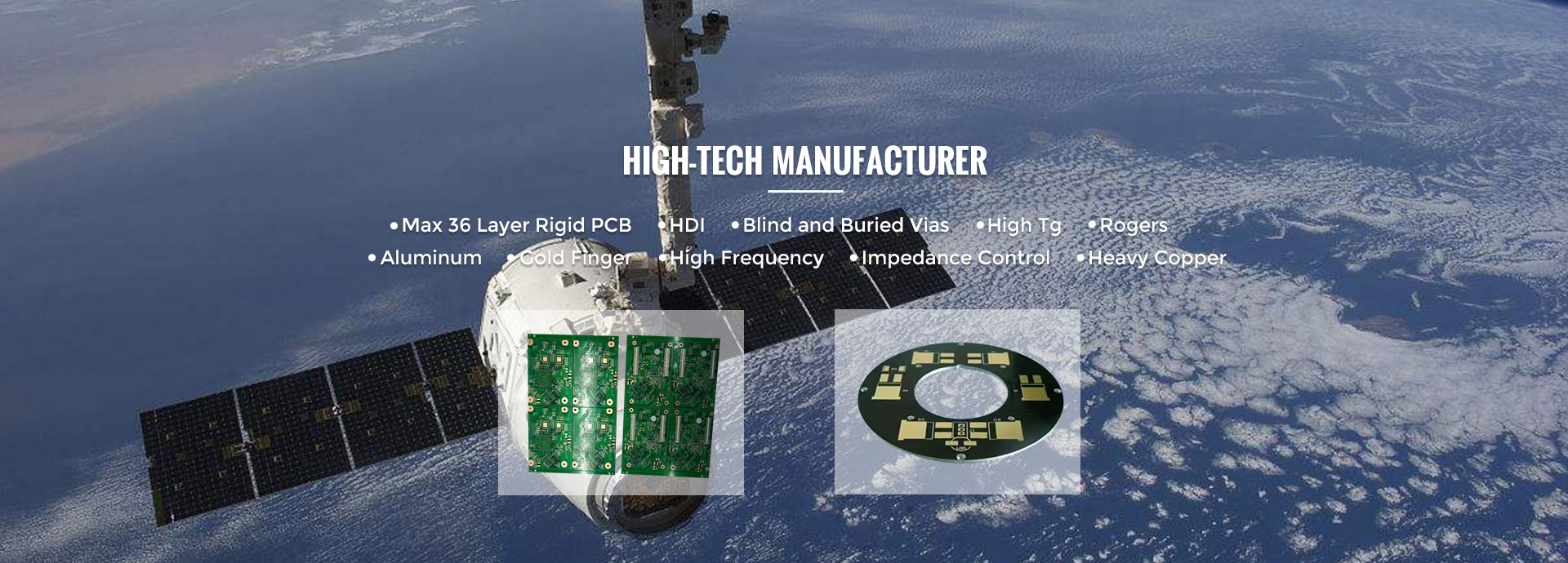
| Technology | Blind and Buried Via, HDI,Hollow out, Selective Hard gold plating,Depth Control,Press fit hole, Edge Half-plated hole, Back drill, Countersink hole, Plated edge, Peelable solder mask, Imedance control, Gold Finger, Fill via with resin and other technology. |
| Materials | Standard FR4/Mid-Tg FR4/Hi-Tg FR4,CEM-1/CEM-3,PTFE,Rogers,Arlon,Taconic,
Teflon,Isola,ITEQ,Dupont,Polyimide,Metal Core Material,Ventec,Nelco |
| Max. PCB Panel Size | 9000mmx820mm |
| Board Thickness | 0.2-12mm |
| Board Thickness Tolerance | ±10% |
| Copper thickness | 0.5 OZ to 22 OZ |
| copper thickness in hole | copper thickness in hole: >25.0 um(>1mil) |
| Min Conductor Line Trace/Space | Inner Layers:≧3/3mil(0.075/0.075mm for 1/2oz base Copper) |
| Outer Layers:≧3.5/3.5mil |
For
Via in Pad | Resin plugged hole size | 0.3-0.75mm |
| Resin plugged board thickness | 0.3-8mm |
| Resin plugged maximum aspect ratio | 40:1 |
| Resin plugged minimum hole to hole space(mm) | 0.65mm |
| For HDI | Min. mechanical drilling hole diameter | 0.15mm |
| Min. laser drilling hole diameter | 0.075mm |
| Max. aspect(micro-via) | 1:1 |
| Max. dielectric thickness for laser drill | 0.05-0.15mm |
| Bottom pad size(under micro-via) | Hole Size+0.17mm |
| Top side pad size(on micro-via) | Hole Size+0.15mm |
| Copper filling | Y |
| Via in pad design | Y |
| Buried hole resin plugged | Y |
| Min. via size can be copper filled | 0.075mm |
| Min plated hole size | 20um(0.8mil) |
| Min Blind/Buried hole size | 0.2mm(8mil) |
| Min Annular Ring | ±0.076mm(±3mil) |
| Min width of cutout (NPTH) | 0.8mm |
| Min width of slot hole (PTH) | 0.6mm |
| Solder mask color | green, red, blue, white, yellow, purple, black, orange, LPI, matt green,matt black |
| Silkscreen color | White, Yellow, Red, Black |
| Surface finish | ENIG, ENEPIG,Immersion Tin, HASL, HASL-LF, OSP,Selective OSP, Gold finger, Immersion Silver,Bare Copper,Hard gold plating, Selective hard gold plating,Selective Immersion gold,Selective gold plating,HASL-LF+Selective Immersion gold,HASL-LF+Selective gold plating,HASL-LF+OSP,and other surface treatments. |
| Outline | Routing, V-cut, Bridge, Stamp hole |
| Outline Tolerance | ±0.15mm (±6mil) |
| Hole Tolerance | PTH +/-3mil |
| NPTH +/-2mil |
| Controled Impendence | +/-5%(<50Ω), +/-10%(≧50Ω) |
| E-Test | Flying probe test:0.4-6.0mm, max 19.6"*23.5" |
| Min spacing from test pad to board edge:0.5mm |
| Min conductive resistance:5Ω |
| Max insulation resistance:250mΩ |
| Max test voltage:500V |
| Min test pad diameter:6mil |
| Min test pad to pad spacing:10mil |
| Max test pad to pad spacing:10mil |
| Max test current:200MA |
| AOI | Orbotech SK-75 AOI:0.05-6.0mm, max23.5"*23.5" |
| Orbotech Ves machine:0.05-6.0mm, max23.5"*23.5" |
| Profiling | Punching,Routing, V-CUT,Beveling |


