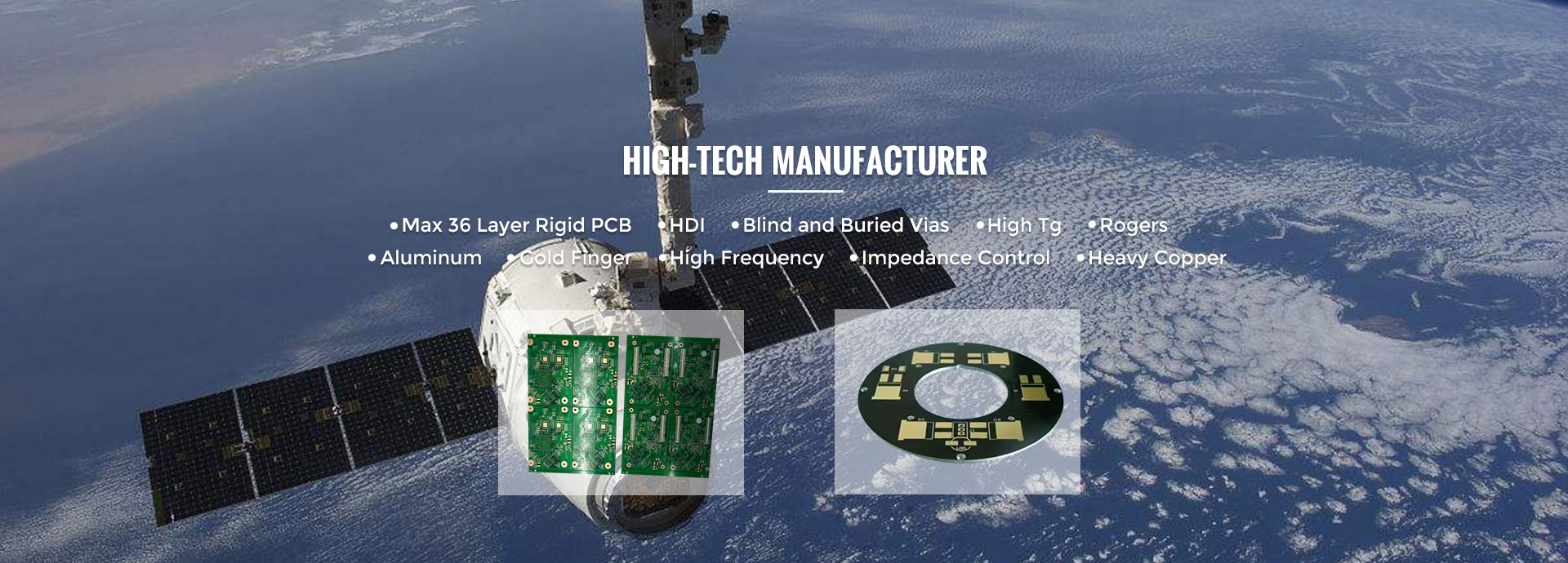
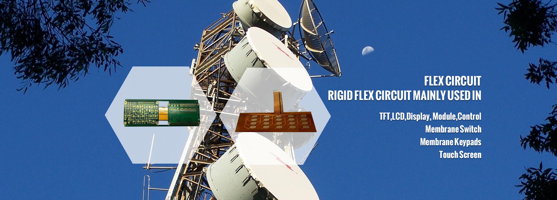
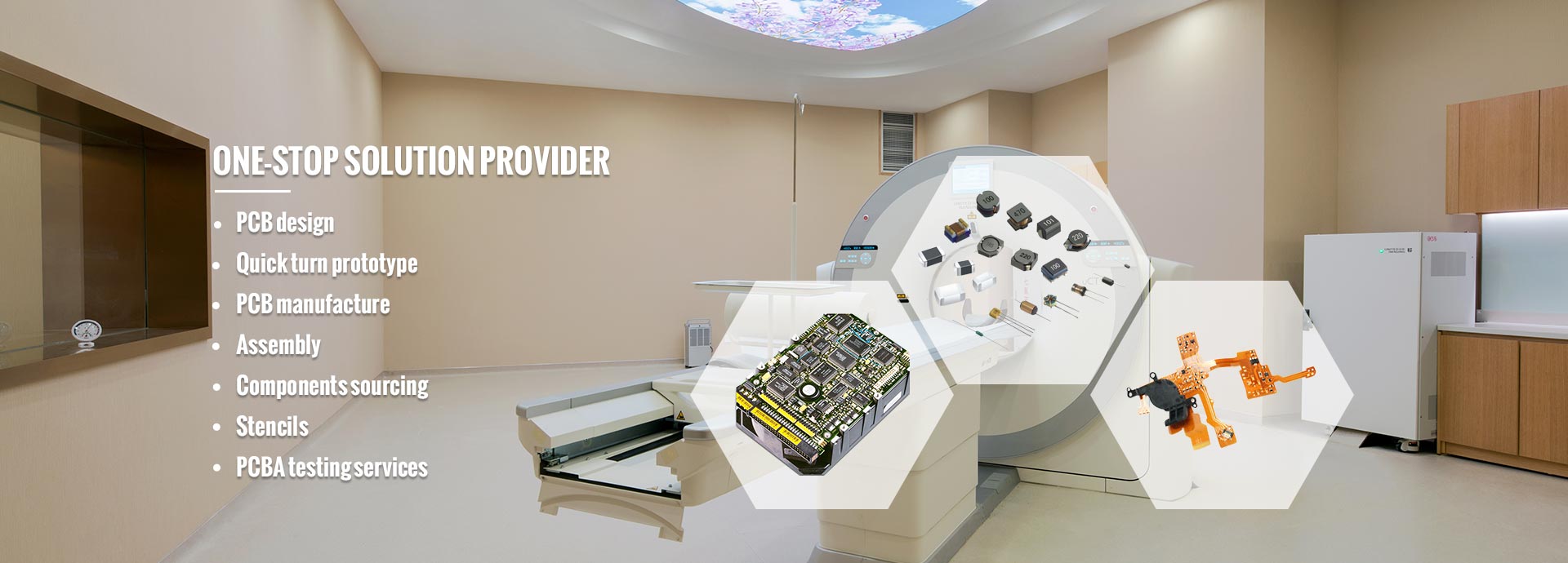
Dear Partners, welcome to MINKINZI – China’s Trusted End-to-End Manufacturing Partner, with 20 years of expertise, we specialize in: Design & Development → Max 58 Layer PCB Fabrication →Turnkey PCBA Assembly → Box-Build Assembly. ODM/OEM/Contract Manufacturing tailored to global standards. Support DFM. Welcome to send your NDA, PCB Gerber, BOM, so that we can provide quotation for you. .
Application:Defense Electronics & Radar Systems
Phased-array radar, electronic warfare (EW) systems
Missile guidance and secure military communication equipment
Primary Drilling: positional accuracy (±2 mil)
Back-Drilling (Controlled Depth Drilling): within ±0.05mm depth accuracy
Multi-Pass Back-Drilling: For ultra-thick boards (≥6mm)
Impedance Control Materials: Use of low-Dk/low-Df high-speed materials
(e.g., Megtron 6/7/8/9, rogers RO4350B, RO4003C)
Description :
Back-drilled via technology is a secondary precision drilling process applied to Plated Through Holes (PTHs) in high-speed, high-frequency PCBs. Using high precision PCB drilling equipment with a specially controlled-depth drill bit, the process precisely removes the unused "stub" portion of the through-hole—the section that does not carry functional signals. The result is a true stubless via PCB structure that delivers superior electrical performance in next-generation systems.
This advanced PCB drilling technology has become a critical enabler for any design operating at multi-gigabit data rates, where every fraction of a millimeter of residual copper can degrade signal quality.
A stub removal PCB is no longer optional in high-speed design—it is fundamental. The core benefits of a properly executed back-drill include:
Eliminates Stub Reflections: Stubs are silent killers of signal integrity. Residual PTH stubs cause standing waves, resonance, and jitter, all of which are eliminated through precise via stub removal.
Reduces Insertion Loss (IL): A low loss back-drill PCB minimizes high-frequency signal attenuation inside the via structure.
Improves Eye Diagram Quality: A well-tuned signal integrity back-drill PCB enhances SI parameters, expanding both eye height and eye width.
Reduces Crosstalk: Especially critical for tightly coupled differential pair routing in high-density designs.
Supports Advanced Materials: Fully compatible with high-speed laminates including M6, M7, M8, PTFE, and LCP.
Executing controlled depth back-drill at production scale introduces several engineering challenges that must be managed rigorously:
Drill Bit Life Management: Precise control of back-drill bit wear is critical to maintaining depth consistency across long production runs.
Z-Axis Depth Control: Achieved through CCD optical alignment combined with real-time depth feedback systems.
Hole Wall Roughness (Ra): Excessive roughness on the back-drilled hole wall can distort high-frequency signals and must be tightly controlled.
Alignment Accuracy: Misalignment between the back-drilled hole and the inner-layer pad must be held within 50 μm to ensure connection reliability.
Selecting a reliable back-drilling partner requires a comprehensive evaluation across six key dimensions. Each of these criteria directly affects whether the finished board will deliver the signal integrity back-drill PCB performance your design demands.
Availability of controlled depth back-drill (CDD) equipment, such as Hitachi, Schmoll, or Weijia CNC drilling machines.
Back-drilling depth tolerance of ±0.05mm or better, with prototype capability at ±0.025mm.
Support for micro-via back-drilling below 0.15mm.
Z-axis alignment accuracy within 50 μm, verified through optical systems.
Demonstrated experience with high precision PCB drilling for both HDI and back-drill hybrid structures.
Familiarity with mid-loss, low-loss, and ultra-low-loss high-speed materials.
Proven experience processing Panasonic M6/M7/M8, SYTECH/ITEQ/EMC, Isola, Rogers, PTFE, and LCP.
Ability to provide tailored back-drilling parameters for different resin systems (CCL/PPE/PPO) to deliver a true low loss back-drill PCB.
Equipped with X-ray thickness gauges to verify residual stub length.
In-house metallographic cross-section analysis capability.
Controllable hole wall roughness (Ra).
Active certifications: ISO 9001, IATF 16949, AS9100, UL, and customer-specific qualifications.
DFM review and back-drilling solution design from early quotation stage.
Signal integrity simulation using HFSS, SI9000, and Ansys SIwave.
Collaborative impedance and impedance control back-drill PCB optimization with customer engineering teams.
Monthly capacity sufficient to support high-volume production ramps.
Clear, predictable lead times for both prototypes and mass production.
Expedited order channels available for urgent engineering samples.
Transparent, tiered pricing structures.
VMI (Vendor Managed Inventory) and JIT (Just-In-Time) delivery options.
Rapid pre-sales and after-sales response, ideally within 24 hours.
Minkinzi has cultivated deep expertise in back-drilled via technology over many years, establishing a mature production system, rigorous quality controls, and a strong portfolio of customer success stories across communications, computing, automotive, medical, and aerospace sectors.
AI Server Accelerator Cards: 1,000+ SKUs delivered; supports up to 58 layers and 112Gbps back-drilling for hyperscale data center customers.
5G RF Boards: Stable supply to leading telecom equipment manufacturers for over five years using advanced PCB drilling technology.
Automotive Millimeter-Wave Radar: IATF 16949 certified; stable production in the 77–79 GHz frequency band for tier-one automotive suppliers.
Data Center High-Speed Backplanes: Volume supply of 400G/800G switch motherboards as a qualified stubless via PCB source.
Military and Aerospace: Fully certified for classified projects; multiple equipment board models have passed final qualification and long-term reliability testing.
Double-Sided Aligned Back-Drilling: Resolves cumulative thickness tolerance issues on large-format boards, ensuring the residual stub is held within specification.
Real-Time CCD Monitoring: In-line depth inspection for every hole location guarantees consistency hole-to-hole and panel-to-panel.
Metallographic Sectioning SOP: Full cross-section inspection of the first article for every new project, validating via quality and via stub removal completeness.
Multi-Drill Bit Life Management: Tracks tool wear across the production run to ensure batch-to-batch consistency on long programs.
Integrated Material-Process-Test Workflow: A seamless end-to-end process from stack-up design through impedance testing, delivering a true signal integrity back-drill PCB for every shipment.
Impedance Engineering Expertise: Dedicated impedance control back-drill PCB engineering support to meet strict differential and single-ended impedance targets for 25Gbps, 56Gbps, and 112Gbps channels.
Whether you are designing a 112Gbps AI accelerator, a 77GHz automotive radar, a 5G mmWave RF front end, or a medical imaging system, the quality of your high precision PCB drilling directly defines the signal integrity of your product. Minkinzi is ready to support you from prototype through volume production with proven stub removal PCB capability and a global customer service team.
Contact Minkinzi Factory for high-precision back-drill PCB manufacturing: Email: sales@minkinzi.com
Applications :
Engineered for high-end electronic sectors including 5G Base Stations, Data Center Servers, AI Accelerator Cards, Network Switches, Core Routers, and Aerospace Avionics systems.
High-precision back-drill technology is engineered to eliminate the "stub" effect that degrades high-speed signal transmission, ensuring superior signal integrity in mission-critical applications. This advanced manufacturing process is widely deployed across the following high-end end products:
Communication and Network Infrastructure — 5G Base Stations including 5G/6G AAU/RRU RF Units with extreme signal integrity requirements; Optical Transceivers in QSFP-DD and OSFP packages spanning 100G, 400G, 800G, and 1.6T configurations; Core Switches and Network Switches with 100G/400G/800G ports featuring dense backplane routing; High-end Router Motherboards supporting Core Routers with multi-port high-speed serial signals; Cloud Computing Servers and Data Center Servers built on AI Server and Cloud Server platforms leveraging PCIe 5.0/6.0 and CXL bus architectures; Data Center high-speed Backplanes; Microwave Backhaul Equipment; Satellite Communication Terminals including VSAT ground station systems; Fibre Channel Switching Equipment; Telecom Baseband Units (BBU); Network Processor Motherboards built on NP and NPU platforms; and Edge Computing Devices requiring low-latency signal performance.
Aerospace and Defense — Military Radar Systems featuring T/R (Transmit/Receive) Modules; Aerospace Avionics System Motherboards for airborne platforms; Phased Array Radar Signal Processing Boards; Electronic Warfare (EW) Equipment; Missile Guidance System PCBs; UAV Flight Control and Video Transmission Motherboards; Satellite Communication Payloads; Military Communication Equipment with encryption capabilities; and Space Exploration Electronics engineered for extreme-environment reliability.
Industrial and Automotive Electronics — Automotive ADAS Modules including millimeter-wave radar mainboards operating at 77GHz and 79GHz; Autonomous Driving Controllers serving as AD/ADAS Central Computing Units; Automotive Ethernet Switches; Industrial automation control boards supporting high-speed industrial buses; High-Speed Oscilloscopes and Vector Network Analyzers (VNA) for precision test and measurement; Medical Imaging Systems including CT, MRI, and ultrasound mainboards; Semiconductor ATE mainboards; and High-Speed ADC/DAC Modules for advanced data conversion applications.
High-End Computing and Consumer Electronics — AI Accelerator Cards and GPU modules including carrier boards for H100 and B200; High-End Graphics Cards; High-End Workstations; High-Performance Computing (HPC) Systems; FPGA Development Boards; NVMe SSD Storage Systems for high-speed storage arrays; AR/VR headset transmission boards; Quantum Computing Controllers requiring ultra-low signal loss; High-Frequency Trading Systems demanding sub-nanosecond latency; Digital Signal Processors (DSP) platforms; Fiber Optic Transmission Equipment; and 8K ultra-high-definition video processing and broadcasting equipment.
High-precision back-drilling is widely recognized as one of the most demanding processes in PCB manufacturing. The following challenges define the technical frontier of this discipline:
Depth Control Precision — Stub length must be controlled within 50μm, with some high-end orders requiring ≤25μm. Drilling speed and feed rate parameters vary significantly based on board thickness, stack-up configuration, and base material properties. Complex depth calculations arise when micro-blind and buried vias are combined with back-drilling operations.
Hole Location Precision — Cumulative interlayer alignment deviation after multiple lamination cycles (≥3 times) must be carefully managed. The concentricity requirement between the back-drilled hole and the target via is ≤0.05mm, which mandates CCD automatic alignment systems and high-precision CNC drilling machines.
Drill Bit Management — Back-drill bits wear out extremely quickly, with a new bit typically processing only 100–300 holes before requiring replacement. Strict control over drill bit runout is essential, as frequent bit changes lead to reduced efficiency, increased costs, and elevated risk of broken bits, residual copper, and rough hole walls.
Signal Integrity Assurance — While back-drilling eliminates the stub effect, it may damage inner-layer copper pads if not precisely controlled. Impedance continuity along the Z-axis signal path must be preserved, and the narrow processing window for high-speed materials (Low-Dk, Low-Df) leaves little margin for error.
Inner Layer and Prepreg Control — Inner-layer copper thickness uniformity directly affects back-drill stop-point detection accuracy. Prepreg (PP) resin flow and filling behavior must be tightly controlled, and resin smear removal inside the hole after back-drilling is critical.
Yield Control Challenges — Initial yield typically ranges from 75% to 90% depending on product complexity. Rework is extremely difficult because back-drilling errors usually result in total scrap. This necessitates 100% electrical testing and cross-section analysis for verification.
Documentation and Traceability — Precise recording of depth and diameter for every hole location is mandatory, and the workload for consistency checks against BOM and Gerber files is substantial. Strict customer requirements for full traceability must be met at every stage.
Equipment-Level Quality Control — CCD-based automatic registration CNC drilling machines (such as Schmoll, Posalux, and Lenz systems) form the foundation of precision drilling. Secondary back-drilling and controlled-depth drilling technology ensures accurate stub removal. Automated Optical Inspection (AOI) provides full coverage of inner layers, outer layers, and solder mask. Automated X-ray Inspection (AXI) verifies BGA, blind/buried vias, and back-drill depth. TDR impedance testers deliver 100% impedance continuity testing. Metallurgical microscopes combined with micro-section analysis enable batch sampling for hole diameter, location, and stub length verification. Flying probe testing and universal fixture testing complete the electrical validation suite.
Process-Level Quality Control — SPC (Statistical Process Control) is applied across drilling, plating, lamination, and solder mask processes. Cpk ≥ 1.33 is maintained for critical processes including hole location, diameter, and impedance. FMEA (Failure Mode and Effects Analysis) covers all high-risk processes. An 8D report rapid response mechanism delivers preliminary reports within 24 hours. A three-stage quality gate system spans Incoming (IQC), In-process (IPQC), and Outgoing (OQA). Supplier audits and incoming inspection are enforced for critical materials including CCL, Prepreg, and chemicals.
System-Level Quality Assurance — ISO 9001:2015 Quality Management System provides the foundational framework. IATF 16949 certification covers Automotive Industry requirements. AS9100D certification addresses Aerospace compliance. UL Certification (UL 796 / UL 94V-0) confirms safety standards. RoHS, REACH, and Conflict Minerals compliance demonstrate environmental and ethical responsibility. A dedicated SPC data-sharing platform is available for customers, and a comprehensive lot traceability system enables traceability from individual boards back to material batches, machines, and operators.
Engineering and Documentation Capabilities — In-depth review of customer Gerber files by CAM engineers ensures manufacturability. DFM reports cover back-drilling feasibility and signal integrity recommendations. Impedance calculation sheets incorporate 3D modeling for accurate prediction. Process parameter records are retained for a minimum of 5 years to support long-term traceability and continuous improvement.
Delivery Capabilities — Standard prototyping lead time is 5–7 days for boards up to 16 layers including back-drilling. Expedited prototyping is available within 48–72 hours for VIP customers. Small-batch lead time is 10–15 days. Mass production lead time is flexibly negotiated based on order volume. Overseas customer support includes multiple trade terms such as DDP, DDU, and EXW.
Flexible Production Capabilities — Flexible switching between high-mix, low-volume orders supports customer EVT/DVT/PVT development stages. Multiple production modes accommodate single boards, small panels, and large panels. A priority channel for urgent orders operates through a dedicated "Hot Lot" mechanism. Vendor Managed Inventory (VMI) options are available for strategic partners.
Production Capacity Assurance — Monthly capacity exceeds 30,000 m² for multilayer boards with back-drilling. The facility is equipped with multiple LDI (Laser Direct Imaging) exposure lines and multiple fully automated vacuum lamination lines. 24-hour shift production is available for specific processes to accelerate throughput when required.
Logistics and Risk Control — Global express delivery is available via DHL, FedEx, and UPS. Vacuum packaging combined with moisture-proof, shock-proof, and ESD protection ensures safe transit. Customs clearance support includes HS codes and CO/AE/EUR.1 certificates. Safety stock is maintained for critical materials, with at least 2 qualified suppliers secured for high-risk materials. Contingency plans address force majeure scenarios including power outages, power rationing, and pandemics.
Communication and Collaboration — A dedicated account manager provides 1-on-1 service for every account. A bilingual (Chinese/English) engineering team ensures seamless global communication. An ERP system enables real-time customer order tracking. Weekly order status synchronization delivers customized reports. 24/7 emergency response is aligned with overseas time zones to support global customers.
If you are seeking a high-end PCB manufacturer with genuine back-drilling capabilities, here is our commitment to your success:
We are more than just a PCB manufacturer — we are your strategic partner in signal integrity for high-end electronics. From initial design reviews to the final details of mass delivery, we safeguard your next-generation products through deep engineering expertise, uncompromising quality standards, and rapid delivery performance. Whether your project involves 5G Base Stations, AI Accelerator Cards, Autonomous Driving Controllers, Aerospace Avionics, Quantum Computing Controllers, or any other demanding high-speed application, our team stands ready to deliver the precision and reliability your designs require.
Welcome to contact Minkinzi for high-precision back-drill PCB manufacturing: Email: sales@minkinzi.com
Flow Chart :
Back-drilling is a precision manufacturing process that removes excess conductive stubs from plated through-holes (PTHs) using a secondary, controlled drilling operation. This advanced technique is essential for high frequency back-drill PCB designs deployed in 5G base stations, hyperscale data center servers, optical modules, aerospace radar systems, high-end core switches, and next-generation telecommunications infrastructure. Untreated stubs generate signal reflections, resonance artifacts, and insertion loss during high-speed signal transmission, directly compromising Signal Integrity (SI) performance. By controlling residual stub length to within 0.05 mm, high-precision back-drilling becomes a critical enabling technology for any back-drill PCB for 5G, back-drill PCB for data center, and back-drill PCB for telecommunications application operating at 25 Gbps and beyond. The same precision discipline applies to every RF back-drill PCB and microwave back-drill PCB used in mission-critical back-drill PCB for aerospace platforms, where signal fidelity is non-negotiable.
The journey begins by collecting complete design data packages, including Gerber, ODB++, and Drill files (.drl/.txt), along with stack-up architecture, back-drilling depth specifications, and impedance targets. Whether the project is an 8 layer back-drill PCB for a network switch, a 12 layer back-drill PCB for a 5G radio unit, or a 16 layer back-drill PCB for an aerospace phased-array radar, the DFM review evaluates alignment accuracy between back-drill holes and target layers, feasibility of stub length tolerance (typically ±0.05 mm; precision up to ±0.025 mm), minimum back-drill hole diameter (≥ 0.2 mm, with ≥ 0.25 mm recommended), minimum safety clearance from back-drill holes to traces and copper planes, stack-up symmetry and lamination thickness tolerance, and impedance continuity together with reference plane integrity.
CAM engineers program drilling sequences covering primary drill, back-drill, and secondary drill operations, then calculate back-drill depth using the validated formula:
Back-drill depth = Total board thickness − Residual stub length − Distance from target layer to board surface
NC files are generated and drilling paths are simulated in software. Engineers also compensate impedance trace width and spacing, while optimizing panel utilization to balance cost and yield across every high frequency back-drill PCB build.
High-speed substrates are selected according to the application's electrical and thermal profile. For 5G and telecom front-haul links, Panasonic Megtron 6 or Megtron 7 are common; for data center backplanes, Isola FR408HR or Hitachi MCL-HS200 deliver outstanding performance; for microwave back-drill PCB and RF back-drill PCB builds, Rogers RO4350B, RO4003C, and Taconic TLY are preferred; for back-drill PCB for aerospace, low-outgassing, high-reliability laminates that meet IPC-4101 slash sheets are mandated. Low-roughness copper foil—RTF (≤ 2 μm) or HVLP (≤ 1 μm)—is required to suppress skin-effect loss. Prepreg (PP) selection must match Tg, Dk, and Df parameters while controlling resin flow. Incoming QC validates thickness uniformity, Dk/Df values, copper foil roughness, and resin content before any material is released to production.
Cutting precision is held to ±0.1 mm, and the material is baked at 150 °C for 2–4 hours to relieve internal stress. Inner layer exposure and etching maintain trace width tolerance at ±0.025 mm (1 oz copper). Inner-layer AOI delivers 100% Automated Optical Inspection, identifying open circuits, short circuits, nicks, and residual copper prior to lamination—essential for the 8 layer back-drill PCB, 12 layer back-drill PCB, and 16 layer back-drill PCB architectures that follow.
Stack-up symmetry is a prerequisite for back-drilling depth accuracy. Vacuum lamination uses optimized pressure and temperature profiles. Dielectric layer thickness tolerance is controlled at ±10%, while total board thickness tolerance after lamination is held at ±5%. X-ray target registration verifies inter-layer alignment at ≤ 75 μm.
High-precision CNC drills from Hitachi, Schmoll, or Via are used to achieve hole position accuracy of ±0.025 mm (4 mil) and hole diameter tolerance of ±0.05 mm. Drilling parameters—spindle speed, feed rate, and entry/backup board selection—are tuned per stack-up. Hole wall roughness is held to Ra ≤ 25 μm, which is vital for any high frequency back-drill PCB destined for 28 Gbps, 56 Gbps, or 112 Gbps channels.
The desmear process combines swelling, MnO4/NaMnO4 oxidation, and neutralization. Electroless copper deposition (0.3–0.5 μm) is followed by panel plating for thickness buildup. Hole copper thickness reaches ≥ 25 μm (IPC Class 2) or 30 μm (Class 3), satisfying the reliability demands of back-drill PCB for 5G and back-drill PCB for telecommunications deployments.
Dry or wet film is laminated, exposed, and developed, then pattern plating builds the final copper thickness (circuit copper plus hole copper). Outer-layer AOI provides a secondary verification step before back-drilling.
This is the heart of every back-drilled build, whether the application is an 8 layer back-drill PCB in a data center NIC, a 12 layer back-drill PCB in a 5G base-station transceiver, or a 16 layer back-drill PCB in a satellite payload.
Equipment Requirements
High-precision CNC drilling machine equipped with a CCD vision alignment system (alignment accuracy ±0.01 mm)
Spindle runout ≤ 0.01 mm
Real-time depth control system with Z-axis resolution ≤ 0.005 mm
Process Parameters
Back-drill bit diameter = Primary drill diameter + 0.15–0.30 mm (0.20 mm recommended)
Back-drill diameter tolerance: ±0.05 mm
Drilling depth is determined by the dual-safeguard approach: Z-axis absolute position control combined with secondary alignment measurement
Recommended method: CCD-based via center detection plus Z-axis bottom-contact sensing
Quality Control
Back-drilled stub length tolerance: ±0.05 mm (high precision: ±0.025 mm)
Back-drill positional deviation: ≤ 0.05 mm
Drill bit life management with first-article inspection every 500 holes per batch
Real-time SPC monitoring of hole position and depth
These tolerances are the reason an RF back-drill PCB can deliver clean 40 GHz performance, and why a microwave back-drill PCB maintains low VSWR across mmWave bands.
Stub removal after back-drilling is followed by desmear and micro-etching. Secondary electroless copper and electroplating reinforcement prevent barrel breakage in back-drilled holes. Outer layer etching and patterning hold trace width tolerance at ±0.025 mm.
Liquid Photo-Imageable (LPI) solder mask is applied, exposed, and developed. Surface finish options include ENIG, Immersion Tin, OSP, Immersion Silver, and Hard Gold. For high frequency back-drill PCB applications, ENIG or Immersion Silver is recommended to minimize signal loss.
CNC or V-Cut profiling maintains dimensional tolerance at ±0.1 mm. 100% electrical testing—flying probe or 4-wire—verifies test point coverage. TDR (Time-Domain Reflectometry) confirms impedance continuity and quantifies stub impact. Impedance testing using TDR or a Vector Network Analyzer is held to ±10% tolerance (±8% for high precision).
Microsection analysis evaluates hole alignment accuracy, actual stub length, hole wall plating quality, dielectric layer integrity, and concentricity between back-drilled and primary drilled holes. X-Ray inspection non-destructively confirms back-drill depth and position. Thermal stress testing at 288 °C (10 s × 3 cycles) ensures no hole wall separation. IST (Interconnect Stress Test) or thermal cycling validates long-term reliability. Customer Signal Integrity testing—eye diagram, jitter, and bit error rate (BER)—closes the loop. Upon approval, the "Golden Sample" is sealed, locking back-drilling parameters for the entire program.
Back-drill Z-value = Total Board Thickness − (Target Residual Stub Length + Target Layer Copper Thickness + Dielectric Layer Thickness) + Process Compensation Value (−0.025 ~ −0.05 mm)
Example: Total board thickness 2.0 mm, signal layer L8, target residual stub 0.05 mm
Back-drill depth = 2.0 − 0.05 − 0.035 (L8 copper + dielectric correction) − 0.03 (compensation) = 1.885 mm
The back-drilling parameter table (BTU table) is standardized, drill bit lifespan and tool-change rules are codified, CCD alignment fiducial design rules are frozen, and the stack-up structure is finalized into a "Golden Stack-up" lock-in. Engineering document version control is managed through a formal ECN process—crucial when scaling an 8 layer back-drill PCB into a multi-line production or transitioning a custom 16 layer back-drill PCB from NPI to volume.
Data is collected across 30–50 consecutive panels (PNL). Critical processes must achieve Cpk ≥ 1.33, with Cpk ≥ 1.67 preferred. FMEA analysis of non-conformities drives PFMEA updates. First-article Cpk verification yield must reach ≥ 98%, ensuring that the back-drill PCB for 5G, back-drill PCB for data center, and back-drill PCB for telecommunications programs can scale without signal-integrity drift.
Equipment cycle time (CT) is calculated, bottleneck processes (typically back-drilling, lamination, and pressing) are identified, and multi-order scheduling is governed by similarity-based priority rules. A dedicated "Hot Lot" process is reserved for urgent orders, including fast-turn prototypes for back-drill PCB for aerospace qualification campaigns.
The full mass production flow proceeds as follows: material release → inner layer fabrication → lamination → primary drilling → PTH (electroless copper) → outer layer imaging → pattern plating → back-drilling → outer layer etching → AOI → solder mask → legend / silkscreen → surface finish → profiling / routing → electrical testing → FQC → packaging and shipping. This sequence is identical whether the build is an 8 layer back-drill PCB for a top-of-rack switch, a 12 layer back-drill PCB for a 5G massive-MIMO radio, or a 16 layer back-drill PCB for a satellite communications payload.
First Article Inspection (FAI) performs a full dimensional check plus cross-sectioning on the first panel of every batch. Patrol inspection cross-sections one panel every 50 panels. AOI/AXI automated inspection covers 100% of the units, and SPC (Statistical Process Control) delivers real-time X-bar/R monitoring. An exception-handling process with line-stop authority and engineer response time under 30 minutes prevents non-conforming material from advancing.
OQC Final Inspection validates appearance, dimensions, hole positioning, copper thickness, and impedance. Packaging uses a vacuum bag with desiccant, bubble wrap, and a corrugated carton for moisture-proof and shock-resistant protection. Certification documents—RoHS, REACH, UL, CQC, and others—are provided with every shipment. On-Time Delivery (OTD) rate is targeted at ≥ 98%.
Minkinzi delivers manufacturing excellence across the full back-drilled PCB portfolio—from compact 8 layer back-drill PCB builds for high-speed networking, to 12 layer back-drill PCB platforms for 5G and telecom infrastructure, to complex 16 layer back-drill PCB architectures for aerospace and defense. Every high frequency back-drill PCB, RF back-drill PCB, and microwave back-drill PCB produced in our facility is governed by the DFM-to-mass-production discipline outlined above, ensuring consistent Signal Integrity, tight impedance control, and reliable long-term performance in back-drill PCB for 5G, back-drill PCB for telecommunications, back-drill PCB for data center, and back-drill PCB for aerospace applications.
Contact Minkinzi today to manufacture your high-precision back-drill PCB:Email: sales@minkinzi.com

Capability :
The fundamental challenge of the back-drilling process lies in the precise removal of the excess "stub." This involves performing a secondary drilling operation—starting from the board surface and proceeding in the opposite direction—on an existing Plated Through-Hole (PTH) to reach a specific target depth (typically resulting in a residual stub of ≤ 10 mils, or even ≤ 5 mils). To achieve consistent, high-quality results, a dedicated PCB manufacturing facility must simultaneously meet a rigorous set of technical conditions.
When it comes to back-drill PCB manufacturing process excellence, every stage—from material selection to final inspection—must be executed with engineering precision. This is especially critical for applications such as back-drill PCB for high speed digital systems, where signal integrity cannot be compromised.
Minkinzi supports a comprehensive range of advanced PCB constructions, including HDI and Any-layer Interconnect designs. Our manufacturing scope includes layer counts ranging from 2 to 56 layers, board thicknesses from 0.2mm to 6.0mm, and maximum board sizes of 610mm × 1100mm. The facility supports full-depth back-drilling, counter-boring, and multi-stage back-drilling configurations. Minimum back-drill hole diameter capability reaches 0.20mm (8 mil), with standard stub control at ≤10 mil and high-precision capability at ≤5 mil (0.125mm).
Our facility is equipped with Hitachi ND Series and Siemens HiCu mechanical drilling machines, including spindles dedicated to back-drilling operations. The German LPKF Lavi Laser Direct Imaging (LDI) exposure system ensures high-resolution imaging for fine-line PCBs. We operate a vacuum resin via-filling line dedicated to Via-in-Pad applications, alongside AMAT/Atotech electroless copper and electrolytic plating lines that deliver surface copper uniformity of ±2μm. Yaskawa (Japan) lamination press systems provide lamination alignment accuracy of ±0.05mm, while Polar/AOI (Automated Optical Inspection) systems and X-Ray Target Drilling equipment are dedicated to back-drilling verification and registration.
Minkinzi's back-drill PCB design support includes impedance control of single-ended and differential pairs at ±5%, with Polar Si8000 impedance calculations and actual impedance coupon test reports. Our mixed lamination capabilities allow hybrid lamination of FR4 with high-frequency materials such as PTFE, Rogers, and Panasonic MEGTRON 6/7. We provide integrated HDI and back-drilling solutions, including Any-Layer HDI (1–3 stages), stacked vias, Via-in-Pad (VIPPO), and back-drilling. Additional specialized options include embedded resistors and embedded capacitors for high-density functional designs.
Every order benefits from end-to-end tracking through dual ERP and MES systems. Safety stock is maintained for common laminates (e.g., S1000-2, ITEQ, Shengyi) to enable rapid material allocation. A 24-hour, 3-shift production mode is available for urgent orders, ensuring that even the most demanding timelines are met without compromising quality.
Minkinzi delivers direct factory pricing with no intermediary markups, positioning us 8% to 15% lower than industry peers. Bulk raw material procurement through strategic partnerships with Shengyi, ITEQ, and EMC ensures controlled material costs. Our specialized HDI and back-drilling pricing structure offers tiered pricing and annual framework agreement rates for high-end PCB clients. Small-batch support is available with a minimum order quantity of just 5 pieces, and prototyping fees can be offset against mass production costs. Flexible payment terms support T/T, L/C, and O/A (30-day monthly settlement available for established clients).
Minkinzi holds comprehensive certifications including ISO 9001, IATF 16949, UL 94V-0, RoHS 2.0, and AS9100D (Aerospace). Our laboratory equipment includes TDR (Time-Domain Reflectometry) impedance tester, DSC (Differential Scanning Calorimeter), TMA (Thermomechanical Analyzer), cross-section micro-etching analysis system, and flying probe tester.
Our end-to-end quality control process follows a strict sequence: Incoming Quality Control (IQC) → In-Process Quality Control (IPQC) and First Article Inspection → Outgoing Quality Control (OQC) → 100% electrical testing and flying probe test prior to shipment. Specialized back-drilling inspection includes 100% X-ray registration check and cross-section sampling for depth verification. Every board features a QR traceability code, providing access to full-process data from raw materials through to shipment. Our quality commitment includes a back-drilling defect rate of less than 0.1%, customer complaint response within 2 hours, and 8D report issuance within 48 hours.
Minkinzi serves as a long-term supplier to leading clients across telecommunications, data centers, automotive electronics, medical, and aerospace sectors. The following case studies demonstrate our expertise in delivering reliable, high-performance back-drill PCB manufacturing process solutions.
This 14-layer design combines FR4 with Rogers 4350B mixed lamination. Back-drilling depth reaches 3.2mm with stub length maintained at ≤8 mils. The project addressed strict high-frequency impedance matching requirements and CTE control for mixed-material lamination. This solution has been validated through mass production supply to a Tier 1 European telecommunications equipment manufacturer.
Designed as a 22-layer board with 2.4mm thickness, this project incorporated 6-layer full back-drilling alongside 4-stage HDI stacked vias. Process challenges included 0.35mm pitch in BGA areas via pitch and precise back-drilling depth control. The boards are now part of the NVIDIA/AMD computing board supply chain.
This 12-layer HDI Any-layer 2nd-order design features full back-drilling of signal channels with stub ≤6 mil. The integrated process highlights HDI via-in-pad, resin plugging, and back-drilling capabilities. This solution is supplied to a Tier 1 supplier for a leading domestic new energy vehicle manufacturer.
This 10-layer design maintains impedance tolerance at ±5% with high signal integrity requirements and stub residue ≤5 mil. The board has passed full IEC 60601 medical safety verification and is designed for long-term stability with a lifespan of ≥10 years.
This 20-layer design incorporates embedded resistors, capacitors, and back-drilling using Polyimide (PI) and High-Tg FR4 materials. The primary process challenge involved via-wall reliability under extreme thermal cycling ranging from -55°C to 125°C. The design carries AS9100D certification and has passed customer second-party audit requirements.
Our 8-layer RF board utilizes Rogers RO4003C combined with FR4, featuring full back-drilling of RF signal vias. The design maintains stable dielectric constant (Dk) with dissipation factor (Df) < 0.003. This technology supports ground terminals for LEO satellite communication and advanced back-drill PCB for radar applications requiring exceptional signal fidelity.
Minkinzi operates a specialized back-drilling line that focuses exclusively on high-end processes such as high-layer-count boards, HDI, mixed-stackup construction, and back-drilling. We are not a generalist shop—our expertise is concentrated where it matters most. Our industry-leading equipment features core drilling and exposure machines less than 3 years old, ensuring a failure rate below 0.5%. Our experienced engineering team includes senior engineers with an average of over 12 years of industry experience, all available to participate in DFM (Design for Manufacturing) reviews. We deliver rapid prototyping and flexible capacity, with 48-hour expedited prototyping options and ample capacity for mass production. Our exceptional value proposition combines high-end quality with mid-range pricing, optimizing your BOM costs. With a proven track record of stable supply to over 500 high-end clients across 30+ countries, our global delivery capability is unmatched.
Whether you require back-drill PCB for high speed digital infrastructure, mission-critical back-drill PCB for military systems, or specialized back-drill PCB for medical devices and back-drill PCB for automotive applications, Minkinzi delivers precision, reliability, and performance at every stage.
Contact Minkinzi today for high-precision back-drill PCB manufacturing:
Email: sales@minkinzi.com
Advantages :
Minkinzi is a professional back-drill PCB manufacturer and back-drill PCB supplier dedicated to the research, development, and production of complex, high-end printed circuit boards. Our core expertise covers high-precision back-drill PCB, HDI PCB, Any-layer HDI, and advanced multilayer back-drill PCB solutions engineered for the world's most demanding industries — including 5G telecommunications, artificial intelligence, automotive electronics, aerospace, and medical devices.
As a vertically integrated back-drill PCB factory, Minkinzi combines more than a decade of CAM engineering experience with cutting-edge equipment to deliver world-class back-drill PCB fabrication and back-drill PCB production services. From rapid back-drill PCB prototype development to large-scale volume runs, we help global customers shorten time-to-market while ensuring uncompromising signal integrity.
Deep Specialization – Minkinzi is 100% focused on advanced PCB technologies, with a particular emphasis on custom back-drill PCB solutions, HDI boards, and Any-layer HDI. This singular focus has made us a recognized back-drill PCB manufacturer trusted by global OEMs and EMS providers.
Experienced Engineering Team – Our CAM engineering team brings over 10 years of hands-on experience in back-drilled PCB design optimization. Every inquiry receives a complimentary DFM (Design for Manufacturability) review, ensuring your high-precision back-drill PCB project is optimized for yield, cost, and performance.
Rapid Response & Quotation – We provide 24-hour DFM feedback and 48-hour engineering quotations for back-drill PCB prototype and production orders, helping you accelerate product launches.
Ultra-Fine Line Width & Spacing – Our back-drill PCB fabrication supports minimum line width and spacing of 2.5/2.5 mil (63.5 μm), perfectly suited for high-density interconnect requirements in 5G, AI, and automotive electronics.
Micro Via Capability – Laser drilling reaches down to 0.075 mm (3 mil), while mechanical drilling achieves 0.15 mm (6 mil), enabling the most intricate back-drilled PCB architectures.
Wide Board Thickness Range – We support board thicknesses from 0.2 mm to 6.0 mm, covering ultra-thin flex-rigid assemblies to heavy copper power boards.
Versatile Copper Weight – Inner layers support H/OZ to 3OZ; outer layers support H/OZ to 6OZ, enabling robust high-current and power-electronics applications.
Broad Layer Count Capability – From 2 layers up to 40 layers, with multilayer lamination tolerance maintained at ±5%. This makes Minkinzi a premier multilayer back-drill PCB manufacturer.
Our mechanical drilling systems deliver hole diameters from 0.15 mm to 6.5 mm, with hole position accuracy of ±0.05 mm (4 mil) and hole wall roughness of ≤25 μm. We routinely achieve aspect ratios (board thickness to hole diameter) of up to 15:1, with the capacity to drill more than 500,000 holes per board — making Minkinzi a high-volume back-drill PCB production partner.
A dual-system configuration combining CO₂ and UV lasers allows us to produce micro-vias as small as 0.075 mm (3 mil) with position accuracy of ±0.025 mm (1 mil) and hole diameter tolerance of ±0.01 mm. Our laser drilling line is qualified for FR4, high-frequency PTFE, Rogers, polyimide (PI), and other advanced materials commonly used in custom back-drill PCB designs.
Back-drilling, also known as controlled-depth drilling, is the cornerstone of our service portfolio. As a specialized back-drill PCB supplier, Minkinzi has perfected this critical process for eliminating signal-degrading via stubs in high-speed designs.
Back-drill stub length controlled to ≤0.05 mm (2 mil) — an industry-leading achievement
Back-drill hole diameter accuracy of ±0.05 mm
Back-drill depth tolerance of ±0.05 mm
Maximum back-drill aspect ratio of 20:1
Back-drill hole count exceeding 10,000 drilled holes per board
Supported layer counts for back-drill boards: 4 to 30 layers
Back-drill alignment via precision X-ray positioning, with offset ≤0.025 mm
Stub control maintained within 50 μm, dramatically improving signal integrity in 25 Gbps+ and beyond applications
This makes Minkinzi a top choice for multilayer back-drill PCB projects requiring tight impedance control, low insertion loss, and superior signal-to-noise performance.
We offer full Any-layer HDI structures including 1+N+1, 2+N+2, 3+N+3, 4+N+4, and 5+N+5 stack-ups, with complete Any-layer interconnection capability (stacked vias, staggered vias, skip vias, and more). Our plated via filling process achieves a fill rate of ≥90%, which is critical for next-generation back-drilled PCB designs.
Our PTH process delivers average barrel copper thickness of 25 μm (1 oz) with a minimum of ≥20 μm. Barrel copper uniformity is maintained with thickness variation between top and bottom of via wall at ≤5 μm, and every board passes Level 10 (10/10) backlight testing.
We offer resin plugging for hole diameters from 0.15 mm to 1.0 mm, achieving a fill rate of ≥95% with dimple depth of ≤0.05 mm on the pad surface. Our vacuum plugging machines combined with thermal curing eliminate air bubbles, and the process is qualified for FR4, high-frequency materials, and rigid-flex boards.
Ideal for HDI Via-in-Pad and VIPPO (Via-In-Pad Plated Over) processes, our copper paste plugging produces a completely flat pad surface suitable for BGA and SMT assembly. Plugging resistance is held to <0.5 mΩ — a key advantage for high-precision back-drill PCB assemblies.
Our green mask plugging achieves a plug depth of ≥75%, with color options including green, white, black, and blue. This process is widely used for BGA pad protection and via protection in back-drill PCB fabrication.
We achieve a fill rate of ≥85% with no dimpling after plating. This process is fully compatible with surface finishes including ENIG, OSP, immersion silver, immersion tin, and electrolytic gold, and supports both stacked and staggered via structures commonly used in back-drill PCB production.
Minkinzi's vacuum press lamination system controls pressure at ≤10 kg/cm², supporting up to 40 layers with dielectric thicknesses from 0.05 mm to 0.5 mm. We work with a full spectrum of materials including Tg130, Tg150, Tg170, Tg180 High-Tg, and halogen-free laminates, achieving layer registration accuracy of ±0.05 mm — essential for multilayer back-drill PCB reliability.
Our imaging line achieves line width/spacing of 2.5/2.5 mil (63.5 μm) with alignment accuracy of ±0.025 mm (1 mil). LDI (Laser Direct Imaging) technology eliminates the dimensional instability issues of traditional film exposure. Laser via diameter tolerance is held to ±0.01 mm, supporting the tightest HDI micro-via requirements.
As a sophisticated back-drill PCB manufacturer, Minkinzi is fully qualified to process advanced RF and high-speed digital materials including Rogers RO4003, RO4350B, RO5880, and RO3003 PTFE laminates, as well as high-speed materials such as M6, MEGTRON 6, FR408HR, and IT-180A. We specialize in hybrid lamination combining high-frequency and FR4 layers, with impedance control maintained at ±5% (typical) and ±8% (limit).
Our rigid-flex capability covers 2 to 20 layers, with flex life exceeding 1 million dynamic cycles. We use both adhesive-based and adhesiveless PI coverlay systems, serving medical, aerospace, and consumer electronics customers worldwide.
Embedded components — embedded chips and embedded resistors
Metal-based boards — aluminum-based and copper-based substrates
Ultra-thick copper — 6 oz to 12 oz power boards
Ultra-thin boards — 0.2 mm ultra-thin core boards
Advanced PCB processes — mSAP and amSAP prepreg replacement for ultra-fine line manufacturing
This comprehensive inspection infrastructure ensures that every back-drilled PCB leaving our factory meets the most stringent quality benchmarks.
IPC-2221 – Generic Standard on Printed Board Design
IPC-2222 – Sectional Design Standard for Rigid Organic Printed Boards
IPC-6012 – Qualification and Performance Specification for Rigid Printed Boards (Class 1 / 2 / 3)
IPC-6013 – Qualification and Performance Specification for Flexible Printed Boards
IPC-6016 – Qualification and Performance Specification for HDI Printed Boards ⭐ Key
IPC-4101 – Specification for Base Materials
IPC-A-600 – Acceptability of Printed Boards (Class 2 / 3)
IPC-TM-650 – Test Methods Manual
IPC-SM-840 – Qualification and Performance of Permanent Solder Mask
IPC-9191 – Statistical Process Control (SPC)
IPC-6016 – Qualification and Performance Specification for HDI Printed Boards ⭐ Core Standard
IPC-6012DA – Automotive Applications Addendum
IPC-9701 – Solder Joint Reliability Test
IPC-9252 – Back-Drilling Stub Control Standard
UL 796 – Standard for Printed-Wiring Boards
UL 94V-0 – Flame Retardancy Rating
RoHS 2.0 (2011/65/EU) – Restriction of Hazardous Substances
REACH (SVHC) – Chemical restrictions
WEEE – Waste Electrical and Electronic Equipment Directive
UL Certification – E-file number (UL Listed)
C-UL / CSA – North American market access
VDE – European electrical safety
CE Marking – EU compliance
CCC – Chinese market (selected products)
ITAR (US Defense Trade) – Military and aerospace sectors
NIST 800-171 – US DoD supply chain (controlled unclassified information)
C-TPAT – Customs-Trade Partnership Against Terrorism
High-Tech Enterprise (China)
"Specialized, Refined, Differential, and Innovative" (SRDI) Enterprise
Green Factory Certification
"Contract-Honoring and Credit-Reliable" Enterprise
Minkinzi stands apart as a back-drill PCB manufacturer, back-drill PCB supplier, and back-drill PCB factory with the technical depth, certifications, and capacity to handle your most demanding projects. Whether you need a fast-turn back-drill PCB prototype, a high-mix custom back-drill PCB run, or full-scale back-drill PCB production for volume programs, our team is ready to support you from DFM review through final shipment.
Our investment in advanced back-drilling equipment, X-ray alignment systems, and process control has positioned Minkinzi as a preferred back-drill PCB fabrication partner for global customers who cannot compromise on signal integrity, reliability, or on-time delivery.
Get a free DFM review and 48-hour quotation for your next high-precision back-drill PCB project.
Email: sales@minkinzi.com Factory: Minkinzi Electronics — Your trusted multilayer back-drill PCB manufacturer
Materials :
Minkinzi — Your Trusted Partner for High-Precision Back-Drill & High-Layer-Count PCB Manufacturing
Specializing in high-precision back-drill PCB manufacturing and deeply experienced in high-layer-count (up to 40L+) technology, Minkinzi delivers professional back-drill PCB solutions and precision back-drill services to high-end sectors worldwide, including telecommunications, data centers, automotive, AI, aerospace, defense, semiconductor testing, and medical industries. As a leading PCB back drilling service provider, we combine advanced controlled depth drilling PCB technology with rigorous depth controlled drilling PCB processes to ensure superior signal integrity, reliability, and performance across every project.
The following PCB types represent our current mass-production portfolio. Each is engineered with optimized back-drill depth control, tight back-drill PCB tolerances, and full compliance with international back-drill PCB specifications:
Additional Engineering Capabilities: Sequential lamination back-drill PCB, any-layer interconnect back-drill PCB, staggered via back-drill PCB, low-loss back-drill PCB, and high-Tg back-drill PCB — all backed by our in-house precision back-drill services and full back-drill PCB assembly support.
Applications: 5G base station AAU/RRU, Massive MIMO antenna back-drill PCB modules, BBU motherboards, RF front-end module back-drill PCB assemblies, power amplifier back-drill PCB substrates, and filter circuit back-drill PCB designs.
PCB Specifications:
Layer Count: 20L–30L
Board Thickness: 2.0–3.5mm
Materials: Mid-loss / Low-loss (Df 0.005–0.012), Rogers material and PTFE-based hybrid stack-ups
Processes: Back-drill PCB assembly with depth controlled drilling to specific layers, hybrid lamination, ±5% impedance control
Special Features: Combination of any-layer HDI back-drill PCB and controlled depth drilling PCB
Customer Value: Signal integrity optimization, SI simulation support, SI test reports provided, plus optimized performance for telecommunication equipment back-drill PCB applications.
Applications: 400G/800G optical modules, core network switch back-drill PCB assemblies, AI accelerator cards, server backplane back-drill PCB designs, and high-speed digital back-drill PCB platforms.
PCB Specifications:
Layer Count: 16L–32L
Board Thickness: 2.5–4.0mm
Materials: Very low-loss (Df 0.001–0.003), M7/M8, with Rogers material options
Processes: Back-drilled vias with stub length ≤75μm, mSAP process, multi-impedance (50Ω/85Ω/92Ω/100Ω)
Special Features: 56Gbps+ PAM4 signaling, PoP (Package-on-Package) support, sequential lamination back-drill PCB construction
Customer Value: Meets high-frequency transmission needs for AI computing cards; back-drill depth control suppresses signal reflection across all data center back-drill PCB builds.
Applications: Avionics systems, radar system back-drill PCB modules, satellite communication back-drill PCB payloads, military communication equipment, and defense-grade electronics.
PCB Specifications:
Layer Count: 16L–40L
Board Thickness: 2.0–5.0mm
Materials: High-Tg back-drill PCB substrates (Tg ≥170°C), PTFE, Polyimide
Processes: Aerospace-grade controlled depth drilling PCB with strict impedance matching, microwave back-drill PCB signal routing
Standards: AS9100, IPC-6012 Class 3
Customer Value: Meets requirements for high reliability and extreme environments, with full traceability for every military-grade back-drill PCB and aerospace back-drill PCB project.
Applications: ADAS controllers, autonomous driving domain controllers, mmWave radar system back-drill PCB, ECU, battery BMS, and antenna back-drill PCB modules.
PCB Specifications:
Layer Count: 8L–20L
Board Thickness: 1.6–3.2mm
Materials: High-Tg back-drill PCB base, low-loss PP, HTC (CAF-resistant)
Processes: Back-drill PCB assembly combined with buried via back-drill PCB and blind via back-drill PCB; automotive-grade reliability
Standards: IATF 16949, AEC-Q100 compliant
Customer Value: Operating temperature -40°C to 125°C; long service life backed by precision back-drill services.
Applications: ATE test boards, Load Boards, Probe Cards, Interface PCBs, and high-speed digital back-drill PCB test fixtures.
PCB Parameters:
Layer Count: 20L–40L+
Board Thickness: 3.0–6.0mm
Materials: Low-loss / Very low-loss, including Rogers material back-drill PCB options
Processes: Ultra-precision controlled depth drilling PCB, deep plating (25μm+), ultra-low roughness copper surfaces, back-drilled vias
Precision: Hole position accuracy ±2mil; line width/spacing 2.5/2.5mil; back-drill PCB tolerances strictly maintained
Customer Value: Meets high-speed signal integrity requirements with extended service life, supported by full back-drill PCB specifications documentation.
Applications: CT/MRI control boards, ultrasound equipment, ECG monitors, wearable medical devices, and RF front-end module back-drill PCB subsystems.
PCB Parameters:
Layer Count: 8L–16L
Board Thickness: 1.0–2.0mm
Materials: Medical-grade FR4, Polyimide (flexible medical)
Processes: Back-drill PCB assembly with rigid-flex integration, controlled depth drilling PCB for signal clarity
Standards: ISO 13485, UL certified
Customer Value: High reliability, miniaturization, biocompatibility, and full compliance with medical device back-drill PCB requirements.
Applications: Industrial PLCs, motion control cards, robot controllers, industrial gateways, and filter circuit back-drill PCB designs.
PCB Parameters:
Layer Count: 8L–20L
Board Thickness: 1.6–3.0mm
Processes: Combination of back-drill PCB assembly, heavy copper, buried via back-drill PCB, blind via back-drill PCB, and stacked via back-drill PCB techniques
Special Features: High-temperature resistance, vibration resistance, long service life with precise back-drill depth control.
Customer Value: Stable 24/7 operation under harsh industrial conditions, with full back-drill PCB specifications provided.
Applications: GPU accelerator cards, AI training modules, edge computing boxes, and high-speed server backplane back-drill PCB platforms.
PCB Parameters:
Layer Count: 20L–32L
Materials: Very low-loss, hybrid material back-drill PCB stack-ups incorporating Rogers material and PTFE-based layers
Processes: High-speed back-drill PCB, mSAP, ultra-low-loss prepreg (PP), microwave back-drill PCB routing
Impedance: 92Ω differential (and other high-speed serial standards), with back-drilled vias optimized for signal integrity
Customer Value: Supports 112Gbps+ signal transmission with industry-leading back-drill PCB tolerances, making Minkinzi the preferred choice for next-generation AI back-drill PCB assembly.
Precision back-drill services with stub length control as tight as ≤50μm
Controlled depth drilling PCB expertise with ±2mil back-drill depth control
Comprehensive back-drill PCB specifications documentation for every build
Full back-drill PCB assembly capabilities from prototype to mass production
Industry-certified quality systems across IATF 16949, AS9100, ISO 13485, and UL
Contact the Minkinzi factory for high-precision back-drilled PCBs: Email: sales@minkinzi.com
Materials :
When signal integrity determines product success, high-precision back-drill PCB technology becomes the decisive advantage. Minkinzi Factory specializes in delivering back-drilled PCB solutions that eliminate stub effects, reduce signal reflections, and ensure optimal performance for 5G, data center, automotive radar, and aerospace applications. As one of the few manufacturers worldwide capable of 100-layer stacking with controlled depth drilling PCB capability, Minkinzi has become the trusted partner for engineers seeking PCB back-drilling service that combines precision, speed, and cost efficiency.
In high-speed digital design, every micron of via stub can degrade signal quality. Our back-drill via PCB manufacturing process removes unused portions of plated through-holes, dramatically reducing parasitic capacitance and improving eye diagram performance. Whether you require custom back-drill PCB designs for prototype validation or multi-layer back-drill PCB production at scale, Minkinzi delivers tolerances of ±2 mil with rapid 1–3 day turnaround.
Our expertise spans HDI back-drill PCB architecture, high-precision PCB manufacturing for telecom infrastructure, and back-drilled via hole PCB fabrication for mission-critical military and medical systems. Every project benefits from our vertically integrated supply chain and direct access to premium laminate materials.
Minkinzi Factory Core Positioning: High-layer-count back-drilling, high-frequency/high-speed capabilities, and 100-layer stacking capability. Recognized as one of the few factories worldwide capable of mass-producing 100-layer PCBs, with strategic focus on high-end sectors including telecommunications, data centers, and automotive radar.
Minkinzi Advantages: 100-layer stacking capability (fewer than 5 manufacturers worldwide can mass-produce this), high back-drilling precision, rapid response, and costs 30–50% lower than Western counterparts. Our high-precision PCB manufacturing capabilities make us the preferred PCB back-drilling service provider for global brands.
Western Advantages: Military/Aerospace certifications, ITAR compliance, and localized delivery.
Southeast Asia Advantages: Low costs and high-volume capacity, but unable to meet high-end back-drilling requirements.
Minkinzi Partnership Model: Capable of handling high-end orders that overflow from Western markets, offering a combination of technical depth and cost efficiency. Whether your project requires multi-layer back-drill PCB complexity, HDI back-drill PCB miniaturization, or custom back-drill PCB engineering, we deliver results that Western suppliers cannot match at comparable cost.
Minkinzi maintains direct inventory and short-lead-time access to the world's leading high-frequency and high-speed materials:
RO4350B
RO4003C
MEGTRON 6 (R-5775)
MEGTRON 7 (R-5785)
MEGTRON 4 (R-5725)
I-Speed (IS620)
Tachyon 100G
FR408HR
N4000-13EP
S7439
These materials are specifically validated for controlled depth drilling PCB processes and back-drilled via hole PCB fabrication, ensuring consistent quality across every production batch.
From initial DFM review to mass production, Minkinzi's engineering team supports your high-precision back-drill PCB project with unmatched technical depth and manufacturing agility. Whether you need a single prototype or volume production of back-drilled PCB assemblies, our streamlined quotation process and dedicated account management ensure your timeline is met.
Contact Minkinzi Factory for high-precision back-drill PCB manufacturing: Email: sales@minkinzi.com
Factory Certified Salt Fog Corrosion Test for Printed Circuit Boards (PCBA) - 48H/96H Reports
Minkinzi Circuit Technology Co., ltd can do Salt Spray Testing & Salt Fog Corrosion Test for our customer's projects. Such as Automotive ...
Unitree Robotics and PCB Technologies: Rigid, Flex, Rigid-Flex, Aluminum, and PCBA
As the main supplier for Unitree Robotics, have high demand for the Rigid, Flex, Rigid-Flex, Aluminum, and PCBA manufacturing, quality and...
Telephone: +86 0769 3320 0710
Cel/What's app: +86 134 6956 5519
Address 1:Songshan Lake International Creativity Design Industry Park,No. 10, West Industrial Road,Songshan Lake High-Tech Dist.,Dongguan,China.523808. Address 2:No. 18, Zhenyuan East Road, Chang 'an Town, Dongguan City, Guangdong Province.523000.