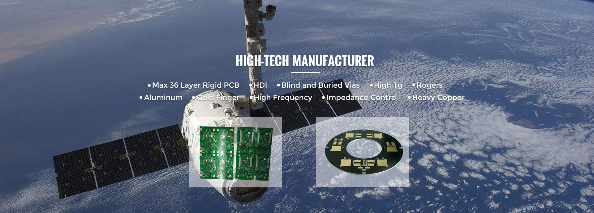
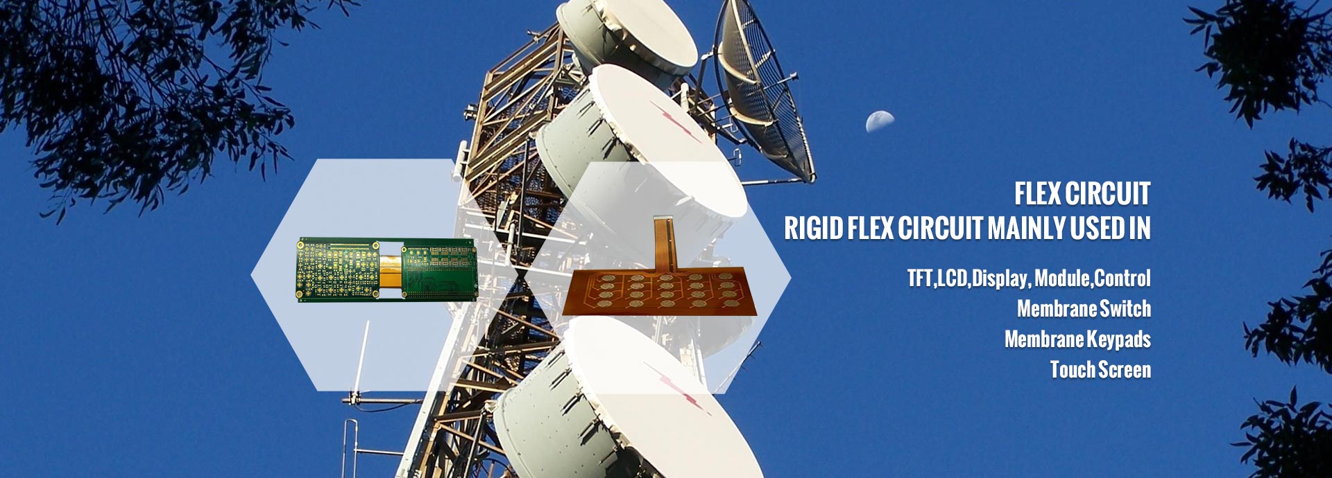
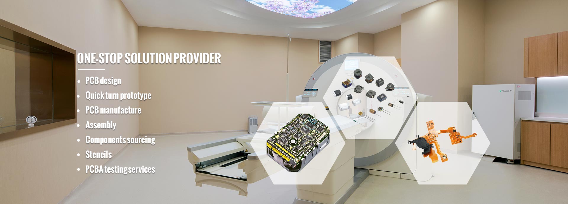
Dear Partners, welcome to MINKINZI – China’s Trusted End-to-End Manufacturing Partner, with 20 years of expertise, we specialize in: Design & Development → Max 58 Layer PCB Fabrication →Turnkey PCBA Assembly → Box-Build Assembly. ODM/OEM/Contract Manufacturing tailored to global standards. Support DFM. Welcome to send your NDA, PCB Gerber, BOM, so that we can provide quotation for you. .
Description :
Oversized PCBs refer to circuit boards whose dimensions exceed the standard PCB size, typically exceeding 600mm in either length or width, or having an area greater than 0.5 m². These circuit boards differ significantly from traditional small-to-medium-sized PCBs in oversized PCB fabrication processes, material selection, equipment capabilities, and design specifications. They represent one of the most technically demanding and comprehensively required sub-sectors in the global PCB manufacturing industry, where specialized knowledge in oversized PCB manufacturing becomes essential.
Large Size: Single board lengths can reach 1m, 2m, or even longer, with LED display wall panels sometimes spanning several meters, making them a benchmark for large PCB production capabilities.
Multi-Layer Architecture: Typically constructed as an oversized multilayer PCB, these boards range from 8, 12, 24, 40 layers or more, supporting complex routing and signal integrity requirements.
Special Materials: Requires high Tg, low CTE (low coefficient of thermal expansion), high heat resistance, and high dimensional stability substrates, including FR-4 high Tg board, BT board, PTFE board, PI board, and ceramic substrate variants.
Complex Processes: Involves thick copper, ultra-thick copper, inner thick copper, special impedance, embedded components, HDI microvias, stepped gold fingers, and mixed pressing techniques that distinguish premium oversized PCB fabrication services.
High Reliability: Applied to high-end fields such as aerospace, military, medical, rail transportation, industrial control, and new energy, where failure is not an option.
LED Display and Lighting (Mini LED/Micro LED display walls, streetlights, tunnel lights)
Industrial Control and Automation
Communication Equipment (5G base stations, satellite communications)
New Energy (photovoltaic inverters, wind power converters, energy storage BMS)
Rail Transit (high-speed rail, subway control boards)
Aerospace (radar, satellite payloads, flight control)
Medical Devices (CT, MRI, ultrasound equipment)
Automotive Electronics (in-vehicle entertainment, ADAS control boards)
Semiconductor Equipment (testing machines, probe stations)
Marine Engineering (ship control, deep-sea equipment)
P0.9 Mini LED 4K/8K Display Wall Mainboard: Size up to 610mm × 457mm, used in ultra-high-definition command centers and TV studios, requiring precision oversized PCB manufacturing tolerances.
Outdoor P10-P20 Full-Color LED Large Screen Mainboard: Size up to 800mm × 400mm, used in stadiums and commercial advertising, a typical candidate for oversized PCB wholesale orders.
Flexible LED Transparent Screen PVC Board: Size up to 1000mm × 250mm, used in commercial windows and stage backdrops, representing fast-growing oversized PCB assembly demand.
Tunnel Light/Street Light Strip PCB: Length up to 1.5m, used in municipal road lighting and ideal for streamlined large PCB production runs.
UV LED Curing Light Source Board: Size up to 600mm × 300mm, used in industrial printing and curing applications.
Photovoltaic Inverter Main Control Board: Size up to 800mm × 600mm, featuring conformal coating and thick copper processes that require expert oversized PCB fabrication.
Energy Storage System BMS Main Control Board: Size up to 700mm × 500mm, multi-layer high-reliability design commonly processed as an oversized multilayer PCB.
Wind Power Converter Power Board: Size up to 1000mm × 800mm, thick copper (6oz-12oz) process demanding specialized oversized PCB manufacturing expertise.
Charging Pile Main Control Board: Size up to 600mm × 400mm, industrial-grade high-voltage withstand design.
HVDC Direct Current Transmission Control Board: Size up to 900mm × 600mm, extra-long size suited to dedicated large PCB production lines.
Nuclear Power Plant Instrumentation Control PCB: Size up to 700mm × 500mm, special substrate, high reliability.
PLC Programmable Controller Mainboard: Size up to 800mm × 600mm, multilayer board configuration.
Industrial Robot Control Board: Size up to 700mm × 500mm, high-speed signal design optimized through advanced oversized PCB fabrication.
SCADA Industrial Monitoring Mainboard: Size up to 1000mm × 800mm, long size configuration.
Semiconductor Wafer Probe Station PCB: Size up to 1200mm × 800mm, high-precision impedance requirements.
AOI Optical Inspection Equipment Mainboard: Size up to 900mm × 600mm, high-speed signal processing.
5G Base Station AAU/RRU Mainboard: Size up to 800mm × 400mm, high-frequency and high-speed materials.
Satellite Communication Phased Array Antenna Board: Size up to 1000mm × 1000mm, millimeter-wave materials requiring premium oversized PCB manufacturing.
Airborne Radar Signal Processing Board: Size up to 600mm × 500mm, high-reliability military-grade construction.
Civil Aircraft Entertainment System Mainboard: Size up to 700mm × 500mm, DO-160 Certification.
High-Speed Rail Traction Control Board: Size up to 1000mm × 600mm, IRIS Certification.
Subway Signaling System Mainboard: Size up to 800mm × 500mm, Safety Integrity Level SIL4.
Vehicle-Mounted HUD Head-Up Display Mainboard: Size up to 600mm × 300mm, Automotive-Grade AEC-Q100.
New Energy Vehicle BMS Main Control Board: Size up to 700mm × 400mm, extra-long size.
CT Scanner Control Board: Size up to 1000mm × 800mm, medical-grade certification.
MRI Mainboard: Size up to 900mm × 600mm, special shielding design.
Deep-Sea Exploration Equipment Control Board: Size up to 700mm × 500mm, high pressure and corrosion resistant.
OLED Evaporation Equipment Carrier Board: Size up to 1200mm × 1000mm, special surface treatment.
Extra-long Flexible Solar Panel (FPC): Length up to 2m, used in photovoltaic roofs.
Data Center Server Backplane: Size up to 1000mm × 800mm, 56-layer ultra-high oversized multilayer PCB configuration.
Choosing a factory capable of producing oversized PCBs requires comprehensive evaluation across multiple dimensions. Whether you want to buy oversized PCB online or establish long-term supply, these criteria matter.
Long Exposure Machine (LDI): Capable of handling lengths exceeding 1.2m.
Long Lamination Machine: Capable of laminating boards exceeding 1.5m in width.
Long Electroplating Line: Capable of achieving uniform electroplating across the entire board.
Long Routing Machine (CNC Cutting Machine): Capable of precisely cutting oversized boards.
AOI/Flying Probe Testing Machine: Supports automated optical inspection and electrical performance testing for oversized boards.
Secondary Support (e.g., immersion nickel-gold, OSP, immersion silver, immersion tin): Ensures uniformity across long dimensions.
These equipment assets directly influence your final oversized PCB price and lead time.
Experience in High Tg Material Applications: Tg ≥ 150℃, 170℃, 180℃.
Special Substrate Supply Capability: High-end materials from Rogers, Isola, Hitachi, Shengyi, and Kingboard.
Mixed-Lamination Technology: Lamination of materials with different dielectric constants (Dk).
Thick Copper Processes: 2oz, 3oz, 6oz, 12oz, 20oz and above.
HDI + Microvia Technology: Laser drilling, through-hole plating.
Impedance Control Accuracy: ±5%, ±8%, ±10%.
Special Surface Treatments: ENIG, ENEPIG, Hard Gold, Soft Gold, OSP, Immersion Silver.
The depth of these capabilities determines the accuracy of any oversized PCB quotation.
UL Certification (UL796 / UL94-V0)
ISO9001, ISO14001, ISO45001
IATF16949 (Automotive)
AS9100 (Aerospace)
ISO13485 (Medical)
IRIS (Rail Transportation)
NADCAP (Special Processes)
DFM Design for Manufacturability: Early involvement in customer design.
SI/PI Simulation Capabilities: Signal integrity, power integrity.
Thermal Simulation Capabilities: Thermal design and heat dissipation solutions.
Reliability Testing: Thermal shock, damp heat aging, HAST, CAF testing.
Rapid Prototyping Capability: Fast delivery time for oversized boards.
Mass Production Capacity: Monthly capacity meeting customer order needs.
Small Batch, Multi-Variety Capacity: Meets diverse customization needs.
One-on-One Account Manager System: Timely response to customer needs.
On-site Technical Support: Available when necessary.
Disclosure Agreement (NDA): Protects customer intellectual property rights.
Global Logistics and Distribution: On-time delivery worldwide.
As a professional manufacturer deeply rooted in high-end PCB manufacturing for many years, Minkinzi Factory has accumulated profound technical expertise and mass production experience in the oversized PCB field, making it a trustworthy partner for global customers who wish to order oversized PCB with confidence.
Equipped with a 1.2m+ LDI ultra-long laser direct imaging machine to meet the high-precision exposure requirements of ultra-large boards, the foundation of precision oversized PCB fabrication.
Possesses a 1.5m+ vacuum laminator to ensure the lamination quality of multi-layer oversized PCBs.
Equipped with an ultra-long PCB production line covering all processes including inner layers, outer layers, solder mask, lettering, routing, and molding, supporting continuous large PCB production.
Possesses an independent high-frequency mixed-pressure lamination production line to meet the special material requirements of aerospace and 5G communication fields.
Minkinzi factory is proficient in the following commonly used materials for oversized PCBs:
FR-4 high Tg substrates: Tg150, Tg170, Tg180, etc.
High-frequency, high-speed substrates: Rogers RO4003, RO4350, RO3003, PTFE, etc.
High heat dissipation substrates: Aluminum substrate, copper substrate, ceramic substrate.
Flexible materials: PI (polyimide), PET, etc.
Special substrates: BT PCBs, Prepregs (PP).
Maximum Board Size: Capable of manufacturing PCBs up to 1200mm × 1000mm.
Maximum Layers: Up to 56 layers as an advanced oversized multilayer PCB.
Thick Copper Process: Supports production of 6oz-20oz thick copper boards.
Impedance Control: Accuracy up to ±5%.
Special Processes: Stepped gold fingers, embedded components, rigid-flex PCBs (RFPC), HDI Any-layer, etc.
Ultra-Long Flexible Boards: Lengths up to 2 meters and above.
Full Turnkey PCB Assembly Services: From sourcing components to final box-build, enabling one-stop oversized PCB assembly.
Minkinzi has provided large volumes of oversized PCB products to customers worldwide:
This proven track record makes Minkinzi a preferred source for oversized PCB wholesale partnerships.
Minkinzi factory has passed multiple international certifications, including UL, ISO9001, IATF16949, AS9100, and ISO13485. A comprehensive quality management system rigorously controls every process from IQC (Incoming Quality Control), IPQC (In-Process Quality Control), OQC (Outgoing Quality Control) to FQA (Final Quality Assurance), ensuring that every oversized PCB meets the high standards required by customers, thereby protecting the long-term oversized PCB price value for our partners.
DFM Team: Involves in the early stages of customer design, providing manufacturability optimization suggestions.
SI/PI Simulation Team: Provides signal integrity and power integrity simulation support.
CAM Team: Possesses experienced CAM engineers capable of handling various complex oversized boards.
Reliability Laboratory: Equipped with thermal shock test chambers, high and low temperature cycling chambers, and damp heat aging chambers.
Minkinzi has established long-term and stable cooperative relationships with numerous customers across Europe, America, Japan, South Korea, Southeast Asia, the Middle East, and Africa. Our products are sold to more than 50 countries and regions worldwide. Customers seeking to buy oversized PCB online can rely on our transparent quotation system, professional engineering team, and dedicated account managers who respond within 24 hours. No matter where customers are located, they can enjoy Minkinzi's professional, efficient, and attentive service.
If you are looking for a high-quality factory that can reliably deliver oversized PCBs at a competitive oversized PCB price with engineering excellence, Minkinzi is your most trustworthy choice! Our Commitment:
✅ Professional: 20+ years of experience specializing in high-end PCB manufacturing; oversized PCBs are our core strength, delivering world-class oversized PCB manufacturing quality.
✅ Reliable: A rigorous quality management system ensures every PCB meets international standards, providing peace of mind with every oversized PCB quotation we deliver.
✅ Efficient: Rapid prototyping capabilities; expedited response time up to 24 hours, making it easy to order oversized PCB prototypes fast.
✅ Flexible: Supports small-batch, multi-variety customization to meet your individual needs, with scalable capacity for full oversized PCB wholesale programs.
Qualified manufacturing partner in China for full turnkey PCB fabrication and assembly of 2-layer, 4-layer, 6-layer, 8-layer, and 10-layer rigid PCBs, plus advanced oversized multilayer PCB solutions.
Full Turnkey PCB Assembly – From bare board fabrication to component sourcing, SMT, through-hole assembly, and final testing, Minkinzi streamlines your entire supply chain.
Top 100 PCB and PCBA Manufacturer Worldwide – Recognized for engineering depth, scale, and reliability across the global electronics industry.
Transparent Online Quotation – Request your detailed oversized PCB quotation with file upload, layer count, material, thickness, copper weight, surface finish, and quantity. Our engineering team responds within 24 hours with a competitive oversized PCB price breakdown, including DFM feedback to optimize manufacturability and cost.
Easy Online Ordering – Whether you want to buy oversized PCB online for prototyping or order oversized PCB in mass production volumes, our digital workflow supports RFQ submission, order tracking, and shipment visibility from quote to delivery.
Welcome to contact Minkinzi factory to manufacture oversized PCBs.
Website: minkinzi.com
Whether your project requires oversized PCB fabrication for aerospace, oversized PCB manufacturing for renewable energy, oversized PCB assembly for industrial automation, or oversized multilayer PCB solutions for next-generation data centers, Minkinzi delivers the scale, precision, and reliability your program demands. Request your oversized PCB quotation today and discover why leading OEMs worldwide choose Minkinzi as their trusted partner for large PCB production.
Applications :
Oversized PCBs refer to circuit boards that exceed the dimensions of standard panels, generally greater than 600mm × 600mm, and extending to 1000mm, 1200mm, or even 1500mm and above. Because of their unique scale, oversized PCBs place exceptional demands on manufacturing processes, equipment capability, quality control systems, and delivery management. Minkinzi specializes in producing oversized FR4 PCB, oversized single-sided PCB, oversized double-sided PCB, large multilayer PCB, oversized rigid PCB, oversized flexible PCB, oversized rigid-flex PCB, oversized aluminum PCB, oversized MCPCB, and heavy copper oversized PCB for the world's most demanding industries.
Large-screen LCD/LED TVs (55 inches and above) — Home theater and commercial large screens
Ultrawide and curved computer monitors — Gaming, financial trading, professional editing
Video wall display systems — Command centers, broadcast studios, retail flagship stores
Interactive whiteboards / Smart boards — Education and corporate collaboration
Digital signage displays — Airports, malls, transit hubs, quick-service restaurants
Large-format LED lighting panels — Architectural lighting, stage backdrops, plant-growth lighting
Industrial PLC (Programmable Logic Controller) systems — Factory automation, process control
CNC machine tool control boards — Precision machining centers
Industrial robot main controllers — Six-axis robots, AGV/AMR main control boards
Semiconductor wafer processing equipment — PCBs inside lithography and etching machines
Automated production line control panels — Smart factory backbone
Large-format printing & copying machines — Engineering copiers, wide-format plotters
EV (Electric Vehicle) central control units — VCU and domain controller boards
EV charging station controllers — DC fast charging pile main boards
Automotive full-length dashboard instrument clusters — Wide cockpit displays
Train / railway signaling control systems — Vehicle signal control boards
Ship & marine navigation control panels — Offshore platform monitoring systems
Solar inverter control boards — High-power string and central inverters
Wind turbine controller PCBs — Main control and pitch system boards
Energy storage BMS (Battery Management Systems) — Commercial and residential ESS
High-power industrial UPS systems — Mission-critical power backup
Smart grid power distribution boards — SCADA monitoring modules
5G base station mainboards — Massive MIMO AAU/RRU RF boards
Server backplanes — AI server and GPU accelerator cards
Data center high-speed switch boards — 400G/800G switch fabric
Satellite communication ground equipment — Ground station receiving systems
MRI / CT scanner control boards — Diagnostic imaging mainboards
Ultrasound & X-ray imaging systems — Medical imaging PCBs
Aircraft cockpit instrument panel PCBs — Avionics display and control
Military radar & electronic warfare systems — Large phased-array radar PCBs
LED advertising display screens (outdoor large screens, stage rental screens)
LED direct display TVs (110 inches and above)
Commercial LCD/OLED display modules (video walls, advertising machines, educational all-in-one machines)
Industrial automation control cabinets (PLC, inverter, servo driver mainboards)
Photovoltaic inverters (high-power string inverters, energy storage converters / PCS)
Wind power converters (main control boards and pitch systems)
New energy vehicle charging pile main control boards
Energy storage battery BMS systems (commercial energy storage cabinet mainboards)
5G base station AAU/RRU and Massive MIMO RF boards
Data center server motherboards (AI server, GPU accelerator card boards)
Semiconductor wafer equipment (PCBs inside lithography machines and etching machines)
Flat panel display manufacturing equipment (FPD production line PCBs)
Medical imaging equipment motherboards (CT, MRI, ultrasonic systems)
Industrial robot control boards (six-axis robot, AGV main control)
CNC machine tool control systems (CNC motherboards, servo drive boards)
Rail transit signaling systems (vehicle signal control boards)
Aerospace ground radar (large phased-array radar PCBs)
Satellite communication ground station receiving system PCBs
Security monitoring splicing screens (video wall matrix control boards)
Intelligent warehousing and sorting equipment (logistics sorting machine mainboards)
Marine engineering equipment (ship control, offshore platform monitoring)
Power grid monitoring equipment (smart grid SCADA systems)
Intelligent transportation ETC systems (highway gantry control boards)
High-end home energy storage (home energy storage main unit BMS)
Large frequency-conversion air conditioner (central A/C main unit control boards)
Industrial UPS (high-power UPS main control boards)
Charging pile liquid-cooling main units (supercharging pile main boards)
Stage lighting control systems (large stage lighting consoles)
High-end audio amplifiers (professional amplifier motherboards)
Large printers / copiers (engineering copier main control boards)
Extra-long Size Production Capability Capable of manufacturing oversized PCBs exceeding 1000mm, 1200mm, and even 1500mm in length. This covers every format from oversized single-sided PCB and oversized double-sided PCB up to high-complexity large multilayer PCB constructions.
Multilayer Board Stacking Capability Mature mass-production of extra-large multilayer boards ranging from 4 layers up to 30 layers or more, with full support for hybrid stack-ups combining FR4, high-Tg, high-frequency, and halogen-free materials.
Special Material Processing Capability Expert processing of high-frequency and high-speed materials, high-Tg materials, PTFE, aluminum substrates, copper substrates, and polyimide — covering oversized FR4 PCB, oversized aluminum PCB, oversized MCPCB, oversized flexible PCB, and oversized rigid-flex PCB on a single platform.
Heavy Copper and Thick Copper Processing Capability Full support for heavy copper oversized PCB constructions with copper weights exceeding 3oz, 6oz, and even 10oz for high-current power electronics, EV charging, and energy storage applications.
Mixed Lamination Structure Capability Mixed lamination of different dielectric layer materials within a single oversized panel, enabling optimized thermal, electrical, and mechanical performance.
Complete International Certifications UL, ISO 9001, ISO 14001, IATF 16949 (Automotive), and AS 9100 (Aerospace) certifications ensure full compliance for global customers.
Strict IPC Standard Implementation Compliance with high-level standards such as IPC-6012, IPC-A-600, and IPC-6013 for every oversized board produced.
Military-Grade Quality Control (where applicable) Full GJB system certification available for defense and aerospace programs.
DFM Review Capability Dedicated DFM rules engineered specifically for ultra-large sizes — including panelization strategy, edge clearance, copper balance, and via aspect-ratio optimization.
CAM Processing Capability Optimization of large board files for paneling design, impedance matching, and thermal design, including CAM350 / InCAM workflows tailored for oversized rigid PCB and oversized flexible PCB builds.
Structural Simulation Capability Thermal simulation, stress simulation, and warpage simulation provided before production to de-risk every NPI build.
Stable Material Supply Strategic partnerships with major material suppliers including Shengyi, Lianmao, Taiguang, Rogers, and Taikangli guarantee consistent material availability for high-mix, high-volume programs.
Rapid Prototyping Capability Expedited delivery in as little as 5–7 days, even for ultra-large boards and 30-layer large multilayer PCB designs.
Stable High-Volume Delivery Capability Monthly production capacity capable of covering the largest customer orders, with redundant capacity on every critical process step.
Cost Control Capability Optimized large-scale production economics for both prototype runs and mass-production programs.
High Yield Advantage Industry-leading yield rates above 96% translate directly into lower hidden costs and faster time-to-market.
Uneven heating across oversized PCBs makes them prone to warpage during thermal stress release. Minkinzi operates dedicated lamination temperature-profile design, multi-stage cooling processes, and warpage control to ≤ 0.75% (industry average 1–2%).
Uneven PP resin flow and inner-layer pattern misalignment significantly increase the risk of layer misalignment at large sizes. Inner-and-outer layer alignment accuracy is held to ≤ ±75μm (8mil), with X-ray drilling and layer-misalignment testing applied to critical builds.
Uneven current density distribution during electroplating of oversized PCBs creates differences in copper thickness across the board surface, edges, and holes. Pulse plating lines and VCP vertical plating lines deliver copper thickness uniformity with surface-to-hole differences ≤ 15μm.
Large boards require extremely high exposure uniformity and resolution. UV-LDI (Laser Direct Imaging) is used in place of traditional exposure machines, achieving line-width accuracy of ±10% across the entire panel.
Drilling large boards is prone to hole-position deviation, broken needles, and rough hole walls. High-precision CNC drilling machines deliver hole-position accuracy of ±50μm across hole diameters ranging from 0.15mm to 6.0mm.
Solder resist printing on large boards is prone to bubbles, uneven thickness, and insufficient exposure. LDI solder-resist exposure ensures solder-mask thickness uniformity within ±5μm.
Large boards are heavy and easily deformed; conventional conveyor belts and fixtures are unsuitable. Minkinzi uses specialized extra-large panel conveyor lines, vacuum-adsorption tables, and operators specifically trained in oversized PCB handling.
Extra-large panels are fragile, easily scratched, and susceptible to moisture. Every shipment uses customized vacuum packaging, shockproof wooden crates, desiccant, and dedicated transportation solutions.
Copper Clad Laminate (CCL): Sampling inspection of Tg value, CTE, and thermal decomposition temperature (Td)
Prepreg (PP): Resin content, gel time, and flowability
Copper Foil: Purity, tensile strength, and elongation
Inner Layer Circuitry: 100% Automated Optical Inspection (AOI)
Lamination: Real-time monitoring of temperature, pressure, and vacuum
Drilling: First-piece confirmation plus in-process sampling
Electroplating: Hourly copper thickness testing plus liquid concentration analysis
Outer Layer Circuitry: AOI plus automated impedance testing
Solder Resistance: Cross-cut adhesion test plus thickness test
Full-size measurement
Warpage test (per IPC standards)
Flying probe test / fixture testing
High-voltage testing (for high-voltage products)
Reliability testing (thermal shock, TCT, HAST) for automotive, medical, and military industries
TDR impedance testing
X-ray hole-deviation inspection
Metallographic section analysis
Thermal stress testing (288°C tin dip)
Ion contamination testing
Unique serial number for every board
Full production process data recording with LOT traceability ≥ 5 years
Full process digitalization via MES system
Monthly Capacity: Extra-large boards ≥ 30,000 m²
Equipment Redundancy: Backup machines configured for every key process
Production Scheduling: APS intelligent scheduling ensures priority for strategic customers
VMI (Vendor Managed Inventory) supported
Batch (JIT) delivery supported
Global logistics offered under DDP / DDU / EXW terms
Real-time order progress query system (customers can log in to view)
Abnormal warning mechanism with 24-hour advance feedback
Photo / video reporting at every key production node
24-hour technical response
48-hour on-site support for strategic customers
Replacement of defective products within 7 days
✅ Extra-Large Size Expertise — Industry-leading capability to manufacture oversized PCBs up to 1500mm × 1500mm, including oversized FR4 PCB, oversized aluminum PCB, oversized MCPCB, oversized flexible PCB, and oversized rigid-flex PCB constructions.
✅ Large Multilayer PCB Leadership — Mature mass production of extra-large boards with 30 layers or more, including heavy copper oversized PCB up to 10oz.
✅ Top-of-the-Line Equipment — LDI exposure, pulse plating, VCP vertical plating, and X-ray target drilling on every critical line.
✅ Stringent Quality Control — IATF 16949, AS 9100, and UL certified, with yield rates consistently above 96%.
✅ Fast Delivery — Expedited delivery in as little as 5 days, with on-time delivery rates above 98%.
✅ One-Stop Engineering Support — Free DFM review plus a dedicated project engineer for every major client.
✅ Global Logistics — DDP / DDU direct delivery to customer warehouses across Europe, the Americas, Southeast Asia, and the Middle East.
Welcome to contact the Minkinzi factory to manufacture Oversized PCBs.Email: sales@minkinzi.com
From oversized single-sided PCB prototypes to large multilayer PCB mass production, from oversized rigid PCB for industrial automation to oversized flexible PCB and oversized rigid-flex PCB for next-generation devices, from oversized FR4 PCB standard builds to oversized aluminum PCB, oversized MCPCB, and heavy copper oversized PCB for power electronics — Minkinzi is your single-source partner for oversized PCB excellence.
Flow Chart :
Oversized PCBs are defined as printed circuit boards with a single panel size exceeding 600mm × 600mm, and often reaching dimensions of 1500mm × 2500mm or larger. These large-format boards are widely deployed across demanding industries including LED displays, 5G infrastructure, renewable energy, industrial automation, and aerospace systems.
Oversized PCB manufacturing presents a unique set of technical challenges that conventional PCB production lines cannot address effectively:
Thermal Expansion Coefficient (CTE) Mismatch — Leading to interlayer cracking during thermal cycling
Uneven Lamination — Resulting in inner layer misalignment across the panel
Large-Area Exposure and Etching Uniformity — Difficult to maintain consistency across meters of surface area
Drilling Position Accuracy Degradation — Particularly in edge regions of large panels
Excessive Warpage Risk — Due to asymmetrical stress distribution
To initiate an oversized PCB project, clients are required to provide: Gerber files, drilling files (Excellon format), stack-up diagrams, PCB specification sheets, and any special process requirements.
Our comprehensive DFM audit focuses on:
Stack-up Structure Rationality — Verifying symmetry of dielectric layer thickness to prevent warpage after lamination
Minimum Trace Width and Spacing — For oversized PCBs, ≥4/4mil is recommended; 8/8mil represents the mass production limit
Hole-to-Trace Distance — Due to significant thermal expansion and contraction, hole rings should be ≥8mil
Panelization Method Optimization — Refining V-CUT, perforated holes, and routing paths to maximize yield
Impedance Control Scheme — Calculating the correspondence between stack-up and trace width while reserving adequate process windows
Critical Process Control: For oversized PCB DFM, the thickness-to-size ratio must be ≥1:100. Separate board design is recommended when this ratio cannot be achieved.
Core Process: LDI (Laser Direct Imaging) is strongly recommended for oversized PCBs to eliminate misalignment problems caused by the expansion and contraction of traditional film, improving alignment accuracy to ±25μm.
Substrate selection is paramount for oversized PCB reliability. Below are our recommendations:
Incoming Material Inspection — Board thickness, copper foil thickness, and glass fiber cloth mesh count verification
Storage Environment — Constant temperature and humidity (Temperature 20±5°C, Humidity 50±10% RH)
Stress Relief Treatment — For oversized boards, post-frame-cutting bake at 150°C for 4 hours is recommended to release internal stress
Process Flow: Cutting → Baking → Lamination → Exposure → Development → Etching → Film Removal → AOI Inspection
Key Process Control Points:
Cutting: Large CNC cutting machines with ±0.1mm sawing accuracy are utilized. Board edges are rounded to R≥2mm to prevent stress concentration during subsequent lamination.
Lamination: Resist dry film (thickness 25–38μm) is applied at 110±5°C with pressure of 0.4–0.6MPa. Bubble and wrinkle prevention is critical, particularly for boards ≥1m.
Exposure: LDI laser direct imaging is preferred as outlined in Stage 2. For traditional exposure methods, double exposure compensation is recommended for oversized boards.
Etching: Acidic copper chloride etching with spray pressure of 2.5–3.0 bar. Etching factor is controlled at ≥3.0. Oversized PCB etching utilizes double-sided synchronous spraying to prevent over-etching.
AOI Inspection: Large-size AOI scanning with segmented defect assessment. Copper leakage, gaps, and excess copper defects are inspected at 100% coverage.
Core Process: Following oversized board inner layer AOI, automatic registration check ensures alignment deviation ≤±50μm.
Lamination represents the most critical and challenging process in oversized PCB manufacturing. The success of the entire build depends on precision control during this stage.
Process Steps: Browning Treatment → Pre-lamination → Lamination → Vacuum Pressing → Post-curing
Key Process Parameters:
Buffer Layer Installation — Silicone pads or kraft paper are added to both top and bottom surfaces of the oversized board to evenly distribute pressure
Slow Pressing Procedure — Multi-stage pressurization prevents transient resin loss
Symmetrical Stacked Structure — Strict symmetry of copper and dielectric layer distribution is mandatory
Post-Curing Treatment — Further resin curing at 175°C for 4 hours following lamination
Core Process: X-ray drilling target inspection is mandatory after oversized PCB lamination. Interlayer alignment must be ≤±75μm (4L–8L) or ≤±100μm (≥10L).
Drilling oversized PCBs introduces several specialized challenges: increased drill bit runout, decreased hole position accuracy, and variation in hole wall quality.
Hole Diameter Accuracy: ±50μm
Hole Position Accuracy: ±75μm (Critical for oversized board edge areas)
Hole Wall Roughness: Ra ≤25μm
Desmear and Etch-back — Ensuring sufficient resin removal from hole walls for reliable metallization
Process Flow: Desmear → Plasma/Etch-back → Chemical Copper Deposition (PTH) → Full Board Electroplating → Pattern Electroplating
Key Process Controls:
Chemical Copper Deposition (PTH):
Hole wall copper thickness ≥0.5μm
Vertical PTH lines are recommended for oversized boards to ensure uniform solution exchange
Back Light Test pass rate ≥95%
Full Board Electroplating:
Current density 2–3 ASD
Oversized PCB electroplating employs pulse plating to enhance deep plating capability
Plating thickness: 20–25μm on board surface, 25–30μm on hole walls
Pattern Electroplating:
Dry film lamination utilizes an automatic laminator to prevent air bubble entrapment
Copper plating thickness tolerance: ±10%
Center-to-edge plating uniformity difference: ≤±15%
Core Process: Following oversized PCB electroplating, thermal stress testing (288°C/10s ×3 cycles) verifies hole wall plating integrity.
The outer layer process flow mirrors the inner layer process, with the additional requirements of solder mask alignment and surface finish preparation.
Key Control Points:
Secondary LDI exposure with ±25μm alignment accuracy
Outer layer etching factor ≥2.8 (ensuring linewidth tolerance)
Diagonal deviation control of oversized boards via 4-corner alignment measurement
Solder Mask Process Options:
Silkscreen Solder Mask (Traditional) — Cost-optimized for standard applications
LPI Liquid Photosensitive Solder Mask (Recommended) — Superior precision for oversized PCBs
Double-Sided Synchronous Silkscreen — Applied for large boards
Solder Mask Thickness — 10–35μm depending on customer requirements
PCB Edge Plating — Oversized PCBs often require edge copper plating combined with solder mask opening
Surface Finish Options:
Key Surface Finish Controls:
Solder mask adhesion: ≥4B (Cross-Cut Test)
Pad solderability: ≥95%
Oversized PCBs require mask bridge strength verification
Oversized PCB Forming Methods:
CNC Routing:
Spindle speed: 30,000–60,000 RPM
Feed rate: 0.5–2 m/min
Sectional cutting recommended for oversized boards to avoid edge chipping from prolonged single milling strokes
V-CUT:
V-CUT angle: 30°/45°, residual thickness 0.3–0.5mm
V-CUT direction must match the pressing direction to prevent delamination
Stamping:
Suitable for high-volume, regularly shaped oversized boards
Die accuracy: ±50μm
Core Process: 100% dimensional measurement via CMM (Coordinate Measuring Machine) ensures external tolerance ≤±0.1mm.
Reliability Testing (Available On Demand):
Thermal Shock (-55°C to +125°C, 100 cycles)
High Temperature and Humidity (85°C/85%RH, 1000 hours)
Thermal Stress (288°C/10s ×3 cycles)
CAF (Conductive Anode Filament) Testing
Final Inspection Process: Appearance Inspection → Dimensional Measurement → Solderability Testing → Pre-shipment Sampling → Vacuum Packaging
Packaging Solution: Oversized boards are protected with multiple layers of pearl cotton, vacuum bags, and reinforced cartons. Moisture-proof bags include humidity indicator cards (HIC). Anti-static packaging is applied for ESD-sensitive devices.
Oversized PCB production lines require independent scheduling to prevent mixing with small-batch products. Equipment OEE ≥85% is considered excellent performance. Single-line monthly capacity reaches ≥8,000m² of oversized boards.
Sample Stage Yield Target: ≥70%
Small Batch Stage Yield Target: ≥90%
Stable Batch Stage Yield Target: ≥95% (Industry-leading level: ≥97%)
Every oversized PCB is equipped with a unique QR code or serial number. The entire manufacturing process is recorded via MES (Manufacturing Execution System), capturing raw materials, equipment used, process parameters, and operator identity. Key processes maintain 100% traceability.
Statistical Process Control (SPC)
Design of Experiments (DOE) for lamination procedure optimization
Regular Cpk analysis to identify special cause variations
Minkinzi specializes in manufacturing oversized LED PCBs for large-format display applications. Our oversized LED PCB and large LED PCB products deliver exceptional thermal management, uniform luminosity, and superior warpage control — essential characteristics for seamless large-format LED video walls, digital signage, and architectural lighting installations.
For linear lighting applications, our oversized LED strip PCB manufacturing capabilities enable extended-length LED strip circuits with consistent impedance, reliable solder joints, and excellent flexibility for both rigid and semi-flex configurations.
When applications demand high current carrying capacity and superior thermal dissipation — such as photovoltaic inverters, power conversion systems, and industrial motor controls — our thick copper oversized PCB capabilities deliver inner layer copper weights up to 6oz and outer layer copper weights up to 12oz. Modified FR-4 substrates with optimized resin systems ensure anti-delamination performance under thermal stress.
For multilayer constructions exceeding 10 layers, our high TG oversized PCB solutions employ Synamic6 or EM-827 substrates with Tg values of 170°C and CTE ≤50 ppm/°C. These materials ensure structural integrity in high-temperature operating environments including under-hood automotive electronics and aerospace systems.
For RF, microwave, and high-speed digital applications, our high frequency oversized PCB and Rogers oversized PCB capabilities utilize Ro4350B and Ro4003C substrates. These low-dielectric-loss materials deliver exceptional signal integrity at frequencies up to millimeter-wave ranges, making them ideal for 5G base station antennas, radar systems, and high-speed data communication infrastructure.
We offer complete surface finish flexibility to match your assembly and reliability requirements:
Oversized PCB with ENIG Finish — Nickel 3–5μm / Gold 0.05–0.1μm, providing excellent solderability and shelf life for BGA and fine-pitch components
Oversized PCB with HASL Finish — Cost-effective lead or lead-free hot air leveling suitable for through-hole and standard SMT applications
Oversized PCB with OSP Finish — Organic solderability preservative coating ideal for short storage cycles and environmentally sensitive applications
Whether you require an oversized LED PCB for a stadium display, a thick copper oversized PCB for a solar inverter, a high TG oversized PCB for aerospace electronics, or a Rogers oversized PCB for 5G infrastructure, Minkinzi delivers engineering excellence from prototype to mass production.
Our engineering team provides complimentary DFM audits within 24 hours, ensuring your oversized PCB project achieves optimal manufacturability, performance, and cost efficiency from the earliest design stages. Partner with Minkinzi — where oversized PCB manufacturing meets uncompromising quality.
Capability :
The production threshold for oversized PCBs (typically referring to single-board dimensions exceeding 600mm × 1200mm, and even reaching 1500mm × 2500mm or beyond) is exceptionally high, far beyond the reach of ordinary PCB factories. A manufacturer capable of producing extra-large PCBs must possess the following core capabilities:
Minkinzi has been deeply engaged in the high-end PCB manufacturing field for many years and has built an industry-leading professional extra-large PCB production line, establishing itself as a trustworthy partner for oversized PCB solutions, including oversized PCB for LED lighting, oversized PCB for power supply, oversized PCB for industrial equipment, oversized PCB for automotive, oversized PCB for medical devices, oversized PCB for aerospace, oversized PCB for telecommunications, oversized PCB for solar inverter, and oversized PCB for UPS applications.
Maximum Board Size: Up to 1500mm × 2500mm (larger sizes can be customized)
Board Thickness Range: 0.2mm – 6.0mm
Copper Thickness Range: Inner layer 1/3OZ – 6OZ; Outer layer 1/3OZ – 12OZ
Number of Layers: 2 – 40 layers (ultra-large multilayer boards)
Minkinzi supports PTFE (Teflon), Rogers, Taconic, Isola, and other high-frequency materials. Our low Dk / low Df material mixing process, combined with high-speed PCB dielectric thickness tolerance controlled within ±5%, makes us a leading choice for oversized PCB for telecommunications, oversized PCB for aerospace, and oversized PCB for LED lighting applications.
mSAP (Semi-Additive Process) Manufacturing Capability
Anylayer HDI (Any-Level Interconnect), with minimum linewidth/spacing of 2mil/2mil
Laser Drilling Minimum Hole Diameter: 0.075mm (3mil)
Mature Via-in-Pad and Through-Pad (BVH) processes
Minkinzi specializes in advanced solutions for oversized PCB for industrial equipment, oversized PCB for power supply, oversized PCB for UPS, and oversized PCB for automotive applications, including:
Buried & Blind Vias (multi-stage stacked vias)
Backdrill accuracy ±2mil
Impedance control ±5%, multi-layer coplanar impedance
Metal substrates (aluminum, copper, ceramic)
Rigid-Flex boards (extra-large size version)
Extra-thick copper foil (Heavy Copper, 6OZ and above)
We offer ENIG (immersion gold), OSP, immersion tin, immersion silver, ENEPIG (electroplated nickel-palladium-gold), hard gold plating, selective immersion gold, lead-free HASL, and leaded HASL — meeting every standard of high-reliability applications, including oversized PCB for medical devices and oversized PCB for solar inverter designs.
✅ Vertically Integrated Supply Chain: Full-chain self-management from raw material procurement to finished product shipment, maximizing cost reduction for oversized PCB for solar inverter, oversized PCB for UPS, and oversized PCB for power supply orders.
✅ Scale Procurement Advantages: Strategic partnerships with international material suppliers such as Shengyi, Kingboard, Rogers, and Taconic ensure lower material costs than the industry average.
✅ Smart Manufacturing Cost Reduction: Investment in MES systems and automated equipment optimizes unit area costs year after year.
✅ Transparent Pricing System: No hidden fees; engineering fees, testing fees, and rush fees are clearly stated.
✅ Long-term Cooperation Rebates: Strategic partners enjoy an annual rebate policy, helping reduce Total Cost of Ownership (TCO).
On-time delivery rate exceeds 98%, with a contractual commitment to compensate for delivery delays — ensuring flawless execution for time-sensitive projects, including oversized PCB for telecommunications rollouts and oversized PCB for automotive production schedules.
ISO 9001:2015 Quality Management System Certification
ISO 14001:2015 Environmental Management System Certification
IATF 16949:2016 Automotive Industry Quality Management System
UL Certification (document number verifiable)
AS9100D Aerospace System (available at select facilities)
RoHS / REACH Environmental Compliance
We apply rigorous quality protocols across every category, including oversized PCB for medical devices and oversized PCB for aerospace:
Incoming Quality Control (IQC): 100% testing of sheet metal, copper foil, ink, and dry film.
Process Quality Control (IPQC): 100% online monitoring of each key process.
Finished Product Quality Assurance (OQA): 100% electrical testing + AOI + visual inspection.
Reliability Testing: Thermal stress testing, IST (Interconnect Stress Testing), Solder Float, Thermal Cycling.
Impedance Testing: Using Polar CITS impedance meter with closed-loop calibration.
AOI Inspection: High-end Orbotech and KLA AOI equipment.
X-Ray Inspection: Used for BGA, buried vias, and back-drilled quality verification.
Flying Probe Testing + Fixture Testing: Double protection ensuring 100% electrical continuity.
SPC (Statistical Process Control): Monitors key process parameters throughout the entire process.
MES System: Traceable production data for each product throughout the entire process.
FMEA/8D Reports: Rapid response to customer feedback with closed-loop improvement.
Minkinzi has accumulated rich practical experience across multiple high-end fields. Below are some representative cases:
Project Background: Supplying 1200mm × 2400mm extra-large PCBs to a well-known international LED display brand. Technical Challenges: Impedance uniformity across extra-long dimensions; COB package gold plating flatness. Solutions: Customized lamination parameters, special electroplating fixture design, Polar CITS impedance closed-loop control. Production Scale: 30,000 units per month with 99.2% yield.
Project Background: Providing a 24-layer high-frequency high-speed mixed-voltage PCB for a 5G communication equipment manufacturer. Technical Challenges: Reliability of the PTFE and FR-4 mixed-voltage interface; ±5% impedance accuracy; 25Gbps high-speed signal integrity. Solution: Utilizing the Rogers RO4350B + RO4450F system with a customized stack-up structure. Certification Result: Passed the customer's full Signal Integrity (SI) verification.
Project Background: Providing a 1500mm × 1800mm large-size carrier board for an international semiconductor equipment manufacturer. Technical Challenges: 12OZ ultra-thick copper heat dissipation layer; ultra-large board warpage control within ±0.5%. Solution: Employing a symmetrical stack-up design, special lamination process, and low-stress curing solution. Application Scenarios: Inside wafer cleaning and etching equipment cavities.
Project Background: Providing an 8-layer, 2nd-order HDI + buried via large-size PCB for a new energy vehicle manufacturer. Technical Challenges: High current carrying capacity (10A continuous), automotive-grade IATF 16949 system compliance, thermal management. Solution: 6OZ thick copper + heat dissipation via array design, with automotive-grade reliability verification. Mass Production Status: Stable mass production for 3 years with zero major quality anomalies.
Project Background: Providing a 16-layer ultra-large-size PCB for a medical imaging equipment manufacturer. Technical Challenges: Medical-grade signal integrity, low noise, long-term reliability (10-year lifespan). Solution: Low-Dk high-speed materials, strict impedance control, 100% X-Ray and AOI dual inspection. Certification Results: Passed the full set of IEC 60601 medical safety standards tests.
Project Background: Providing 20-layer PTFE high-frequency PCBs for an aerospace research institute. Technical Challenges: Extremely low loss (Df < 0.0025), vacuum environment venting control, aerospace-grade reliability. Solution: All-PTFE system, special degassing process, ultra-clean environment packaging. Special Requirements: NADCAP or special military standard certification support can be provided according to customer requirements.
Project Background: Supplying ultra-large size + rigid-flex board to a global industrial robot brand. Technical Challenges: 12-layer Rigid-Flex integration, 1 million bend cycles lifespan. Solution: Using Adwill glue-free flexible board material, 0.2mm PI protection window. Mass Production Status: 25,000 pieces per month.
Project Background: Supplying 1500V system-level ultra-large-size PCBs to a leading photovoltaic company. Technical Challenges: 12OZ thick copper, high current (300A+), high CTI withstand voltage, outdoor weather resistance. Solutions: High Tg (TG170+) materials, high CTI materials, special solder mask design.
From engineering assessment → CAM production → manufacturing → component procurement → assembly (PCBA) → testing → global logistics, our end-to-end one-stop service saves you time and effort across every product category — from oversized PCB for power supply and oversized PCB for UPS to oversized PCB for solar inverter and oversized PCB for automotive.
Our products are exported to North America, Europe, Japan, South Korea, Southeast Asia, Australia, the Middle East, and other regions. Our clients include Fortune 500 companies, leading industry brands, listed companies, and research institutions.
We invest over 5% of our revenue in R&D annually, keeping abreast of cutting-edge industry technologies (mSAP, IC Substrate, millimeter-wave radar, etc.) and growing together with you.
1-on-1 Dedicated Account Manager for Full Support
Free DFM Inspection (Manufacturability Analysis)
24-Hour Technical Support
Global Express Door-to-Door Service
Welcome to contact Minkinzi factory to manufacture oversized PCBs — including oversized PCB for LED lighting, oversized PCB for power supply, oversized PCB for industrial equipment, oversized PCB for automotive, oversized PCB for medical devices, oversized PCB for aerospace, oversized PCB for telecommunications, oversized PCB for solar inverter, and oversized PCB for UPS.
Advantages :
Layer Range: 16, 20, 24, 30, 40, 50 and above
Core Processes: High alignment lamination (±25μm), ultra-thin core board (0.05mm), high-speed material lamination
Application Scenarios: Core routers, AI accelerator cards, supercomputer motherboards
Structure Types: 1+N+1, 2+N+2, 3+N+3, Any-layer (any-layer interconnect)
Core Processes: Laser-drilled blind vias/buried vias (diameter ≤75μm), micro-line width/spacing (3mil/3mil), mSAP process
Application Scenarios: 5G mobile phone motherboards, smart wearables, IoT modules
Structural Features: Multi-layer rigid board and flexible area integrated lamination
Core Processes: PI film lamination, window opening, impedance consistency control
Application Scenarios: Aerospace electronics, medical implant devices, foldable screen modules
Material Systems: Rogers, Taconic, Panasonic MEGTRON, Isola, Nelco
Core Processes: Precise dielectric constant (Dk) control, low loss (Df≤0.002), PPO/PPE resin system
Application Scenarios: Millimeter-wave radar, base station antennas, 800G optical modules
Copper Thickness Range: 3oz, 4oz, 6oz, 10oz, 12oz to 20oz
Core Processes: Uniformity of thick copper plating, heat dissipation design, lamination bubble control
Application Scenarios: Industrial power supplies, new energy inverters, rail transit traction
Process Features: Resistors, capacitors, and chips are embedded within the PCB
Core Processes: Flatness of embedded components, connection reliability
Application Scenarios: Power modules, automotive ECUs, medical devices
Structure: Aluminum substrate, copper substrate, AlN/Al₂O₃ ceramic substrate
Core Processes: High thermal conductivity (1W/mK ~ 170W/mK), thermal resistance control
Application Scenarios: High-power LED lighting, laser devices, IGBT modules
Process Features: Fine lines (≤15μm), small apertures (≤50μm), high flatness
Application Scenarios: High-end chip packaging, AP/CPU packaging substrates
Size Range: Single board size up to 1200mm × 600mm or larger
Core Processes: Uniformity of large PCB lamination, no deformation of inner layer patterns, consistent impedance over ultra-long lengths
Application Scenarios: Communication base station backplanes, data center switching matrices
Including Cavity boards, Copper Coin boards, Semi-Flex boards, and ultra-thin boards (0.2mm), etc.
Core Processes: Controlled depth milling, copper coin lamination, laser forming
As a trusted giant PCB manufacturer, Minkinzi has delivered high-reliability large PCB board solutions across the most demanding industries worldwide. Our extra large PCB expertise is validated through every jumbo PCB project we complete.
When customers search for a reliable large format PCB manufacturer, they consistently choose Minkinzi for our proven ability to deliver big PCB solutions at scale. Whether you require an oversized printed circuit board for telecommunications backplanes or a large printed circuit board for AI server infrastructure, our facility is purpose-built for extra-large production.
Maximum Board Size: 1200mm × 600mm (Larger sizes available upon request) Maximum Layers: 50+ Maximum Board Thickness: 8mm Minimum Board Thickness: 0.2mm
As a leading jumbo PCB supplier, Minkinzi specializes in large PCB board fabrication that exceeds standard industry dimensions, ensuring your most ambitious designs can be manufactured as a single integrated unit rather than split across multiple boards.
✅ Distortion-Free Exposure of Large-Size Inner Layer Patterns (LDI Laser Direct Imaging)
✅ Uniformity of Ultra-Long Size Lamination (Hydraulic/Vacuum Lamination)
✅ Uniformity of Large Thick Copper Plating (Electroplating Uniformity ≥90%)
✅ Ultra-Long Impedance Consistency (Impedance Tolerance ±8%)
✅ Large-Size AOI/X-Ray Inspection Capabilities
✅ Oversized PCB Warpage Control (≤0.75%)
Our giant PCB production lines are engineered to handle the unique challenges of large format PCB manufacturing, including thermal management during lamination, pattern registration across expansive areas, and maintaining signal integrity across extended trace lengths.
✔ Free DFM Inspection
✔ High-Speed, High-Frequency PCB Signal Integrity (SI) Simulation Support
✔ Impedance Modeling and Stack Design Optimization
✔ One-Stop PCBA Assembly (Including SMT, Testing, BOM) (Matching Available)
Up to 50 Layers | 1200mm × 600mm | Full Turnkey Solutions
When your project demands an oversized PCB that pushes the boundaries of conventional manufacturing, Minkinzi delivers the engineering depth, equipment capacity, and quality certifications to bring your design to life. From prototype to mass production, our team supports every stage of your large printed circuit board journey with free DFM reviews, signal integrity simulation, and one-stop PCBA assembly.
Welcome to contact Minkinzi factory to manufacture your oversized PCB, large PCB, big PCB, large printed circuit board, oversized printed circuit board, large format PCB, extra large PCB, giant PCB, jumbo PCB, or large PCB board requirements.Email: sales@minkinzi.com
Materials :
An oversized PCB refers to a printed circuit board whose dimensions exceed the standard PCB manufacturing range, typically surpassing 24"×24" (610mm×610mm) and often reaching 1.5 meters or even beyond 2 meters. As a leading oversized PCB manufacturer, we recognize that these boards are engineered for mission-critical large-scale systems where reliability, dimensional stability, and high-speed performance are non-negotiable.
An oversized PCB, also commonly referred to as a large PCB panel, big size PCB, or large size PCB, is defined by several distinguishing characteristics:
Exceptional Dimensional Scale: Length or width significantly exceeds the processing limits of conventional PCB equipment, requiring specialized handling and fabrication infrastructure. Our non-standard size PCB capabilities allow us to deliver truly custom solutions for unique applications.
Flexible Layer Architecture: Layer counts range from simple 2-layer designs to highly complex stackups exceeding 40 layers, supporting diverse signal integrity and power distribution requirements.
Advanced Material Selection: We primarily utilize specialty substrate materials with high Tg, low CTE, and low loss characteristics—including modified FR4, PTFE, ceramic-filled substrates, PPO, and modified epoxy systems—sourced from premier manufacturers such as Shengyi Technology, Taikuang Electronics, Panasonic, Rogers, and DuPont.
Sophisticated Manufacturing Processes: Production involves specialized lamination, precision electroplating, ultra-long trace compensation, and high-density interconnect (HDI) techniques that go far beyond conventional PCB workflows.
Mission-Critical Applications: Oversized PCBs serve as foundational components in advanced communication infrastructure, rail transit systems, aerospace platforms, new energy installations, and next-generation computing systems.
As a trusted oversized PCB supplier and oversized PCB factory, we serve an extensive range of industries requiring custom oversized PCB solutions. Below are thirty typical application scenarios where our large format PCB expertise delivers tangible value.
5G Base Station Equipment: Ultra-large backplanes and mainboards for Massive MIMO antenna systems, supporting the high-frequency, high-bandwidth demands of modern wireless infrastructure.
6G Pre-Research Equipment Mainboards: Ultra-large motherboards engineered for millimeter-wave and terahertz communication prototypes.
Satellite Communication Systems: Large signal processing PCBs for ground stations and space-based communication platforms.
Submarine Optical Cable Repeaters: High-reliability large PCBs designed for harsh undersea environments and long-term deployment.
Network Switches & Routers / Server Backplanes & Data Center Hardware: Motherboards for high-port-count switches and supercomputer interconnect backplanes supporting hyperscale data center operations.
Supercomputing Center Backplanes: High-layer-count, high-speed interconnect boards for next-generation HPC systems.
Radar Systems: Phased array radar substrates and signal processing boards for both civilian and defense applications.
Broadcast Television Transmitter Mainboards: Motherboards for high-power transmission systems delivering reliable broadcast performance.
Quantum Communication Equipment Mainboards: Specialized boards for quantum key distribution equipment requiring ultra-precise signal integrity.
AI Training Cluster Backplanes: High-density motherboards for GPU cluster systems powering artificial intelligence workloads.
Railway Signaling & Control Systems: High-speed train control mainboards for traction and braking control systems, fully compliant with EN50155 rail transit standards.
Subway Signaling Mainboards: CBTC signaling system mainboards delivering fail-safe communication for urban metro networks.
Electric Vehicle (EV) Battery Management Systems (BMS): Whole-pack battery management mainboards utilizing 2oz thick copper and buried via technology to carry high current reliably.
Automotive Infotainment Systems: Central computing unit mainboards integrating entertainment, navigation, and connectivity features.
Intelligent Driving Domain Controllers: Advanced mainboards serving as central computing platforms for autonomous driving architectures.
EV Charging Stations: High-power charging module main control boards supporting fast-charging infrastructure deployment.
Marine Navigation & Control Electronics: Ruggedized mainboards for marine vessels and offshore platforms operating in corrosive saltwater environments.
Civil Aircraft Avionics System Mainboards: Flight control computer mainboards engineered to meet rigorous aviation reliability standards.
Military Communication Equipment: Electronic warfare system boards supporting secure tactical communications.
UAV Ground Station Mainboards: Command and control center boards for unmanned aerial vehicle operations.
Spacecraft Power Management Boards: Satellite power system mainboards meeting strict space-grade qualification requirements.
Missile Launch Control Mainboards: Weapon control system boards meeting MIL-PRF-31032 military specifications.
Surveillance & Security Control Panels: Mainboards for advanced security monitoring and threat detection systems.
Solar Inverters: High-power photovoltaic grid-connected inverter main control boards optimized for renewable energy conversion.
Wind Turbine Controllers: Megawatt-level wind power converter mainboards delivering reliable performance in demanding environmental conditions.
Industrial Power Supply Units (PSUs): Robust mainboards for industrial-grade power conversion and distribution.
Smart Grid Equipment: Power protection system relay mainboards supporting intelligent grid infrastructure.
Uninterruptible Power Supplies (UPS): Mainboards ensuring continuous power delivery for critical load protection.
Industrial Control Systems (PLC): Multi-axis motion controller mainboards supporting complex automation sequences.
CNC Machine Control Boards: Precision mainboards driving computer-controlled machining equipment.
Robotics Main Control Boards: Advanced mainboards for industrial robots and collaborative automation systems.
Factory Automation Equipment: Mainboards supporting fully integrated smart manufacturing lines.
Industrial Printers / Printing Machinery: Specialized control boards for high-throughput commercial and industrial printing operations.
CT / MRI / Ultrasound Imaging Systems: Large medical imaging equipment mainboards supporting diagnostic accuracy and patient safety.
Medical Diagnostic Equipment: Mainboards for advanced clinical diagnostic platforms.
Laboratory Test & Measurement Instruments: Precision mainboards for high-energy physics experimental equipment and particle accelerator control systems.
LED Video Walls / Advertising Displays: Driver boards for large-format outdoor and indoor LED video walls and digital signage installations.
Large-Screen LCD/TV Backlight Units: Driver boards supporting high-brightness commercial display backlighting.
Commercial LED Lighting Panels: Driver boards for architectural and commercial LED lighting installations.
Digital Signage & Kiosks: Mainboards powering interactive kiosks and digital advertising displays.
Smart Home / Building Automation Control Panels: Intelligent control mainboards for residential and commercial building management systems.
Selecting the right custom oversized PCB partner requires careful evaluation across multiple critical dimensions.
Equipment Capabilities
Customers should verify whether the manufacturer possesses ultra-large vacuum presses (such as hot presses exceeding 2 meters), ultra-long exposure machines (LDI or traditional exposure equipment) capable of solving large-format alignment challenges, gantry automatic electroplating systems delivering uniform plating thickness, and ultra-long CNC milling machines for precise mechanical fabrication. As an experienced oversized PCB factory, we have invested substantially in all these capabilities.
Materials and Processes
Evaluate whether the manufacturer maintains reserve stocks of large-size specialty substrates from premier brands (DuPont, Taikuang, Shengyi), possesses low-loss high-speed material processing expertise (Rogers, Panasonic MEGTRON series), demonstrates experience in complex multi-lamination processes (boards exceeding 20 layers), and delivers precise impedance control (±5% or ±10% accuracy). Our custom large PCB services routinely support all these demanding requirements.
Quality Control
Confirm whether the manufacturer is equipped with large-format AOI (Automated Optical Inspection) scanning capability, possesses X-RAY and cross-section analysis capabilities for failure analysis, and holds essential certifications including UL, ISO9001, IATF 16949, and AS9100.
Delivery and Service
Assess whether the manufacturer offers specialized packaging and transportation solutions for large-size PCBs (anti-warping, anti-collision protection), rapid NPI (New Product Introduction) response, strong engineering support through experienced CAM engineer teams, and comprehensive one-stop service covering PCB fabrication, component sourcing, and full assembly.
Equipment Investment
Our facility is equipped with a 2.4-meter ultra-large vacuum press capable of meeting lamination requirements for boards exceeding 1.5 meters. We operate double-tablet ultra-long exposure machines specifically designed to solve large-format alignment challenges. Our gantry automatic electroplating system delivers plating uniformity within ±10%. We also maintain large reflow lines and tin spraying lines fully adapted to large board surface treatment requirements.
Material Inventory Stockpiles
We maintain regular stock of large-size substrates including FR4, high-Tg FR4, PTFE, PPO, and modified epoxy materials. We have established strategic partnerships with premier material manufacturers including Shengyi Technology, Taikuang Electronics, Panasonic, and Rogers. Our maximum board material dimensions reach 1500mm × 2000mm, enabling true custom size PCB flexibility.
Process Expertise
Our cumulative deliveries exceed 50,000 square meters of oversized PCB production. We proudly serve clients across 5G communications, new energy, rail transit, and aerospace sectors. Our maximum layer count exceeds 40 layers, and our minimum line width/spacing capability reaches 3mil/3mil (0.075mm)—among the most advanced in the industry.
5G Base Station Project
We supplied 900mm × 600mm 28-layer backplanes for a major international telecommunications company. Our team successfully solved the warpage challenges associated with ultra-large-area M6 high-speed material lamination, achieving warpage control within 0.5%.
New Energy Vehicle BMS Project
We delivered 800mm × 400mm 12-layer battery management mainboards featuring 2oz thick copper and buried via technology to carry high current reliably. All products passed IATF 16949 automotive system certification.
Rail Transit Project
We provided 1200mm × 800mm 20-layer control mainboards for high-speed rail clients. These boards fully comply with EN50155 rail transit standards and successfully passed severe temperature cycling tests ranging from -40°C to +85°C.
Aerospace Project
We supplied military radar 1500mm × 1000mm 16-layer high-frequency high-speed boards. These products meet MIL-PRF-31032 military standards and have passed GJB military system certification.
Every board undergoes 100% AOI inspection, flying probe testing, and impedance testing before shipment. Our CAM engineering team provides 24-hour rapid response to all customer inquiries. We offer complimentary DFM (Design for Manufacturability) analysis to optimize your designs for manufacturability. Our surface treatment options include V-CUT, stamp hole, immersion gold, OSP, and tin spray processes. All shipments are packaged using anti-static vacuum bags, pearl cotton cushioning, and reinforced wooden crates to ensure safe delivery.
We support worldwide shipping through DHL, FedEx, sea freight, and air freight channels. Our multilingual customer service team provides native support in Chinese, English, Japanese, and German. We offer expedited prototyping with delivery in as little as 5-7 days for urgent oversized board requirements. Standard bulk delivery typically requires 10-15 working days. We support low-volume production with flexible minimum order quantities—even single-piece prototypes are welcomed.
Whether you require a large PCB panel for LED video walls, a big size PCB for industrial automation systems, or a fully custom oversized PCB for aerospace applications, Minkinzi Factory stands ready to deliver. Our combination of advanced equipment, premium materials, rigorous quality control, and dedicated engineering support makes us the oversized PCB supplier of choice for demanding global customers.
Contact us today to discuss your oversized PCB requirements: Email: sales@minkinzi.com
Let our expertise in large size PCB manufacturing power your next breakthrough innovation.

Materials :
Welcome to the most comprehensive technical guide on high-end PCB substrate materials and global production capacity benchmarking. This resource has been engineered for design engineers, procurement leaders, OEM/ODM decision-makers, and EMS partners who demand clarity when selecting materials, evaluating manufacturers, and commissioning oversized PCB projects for mission-critical applications.
The FR-4 family remains the industry's workhorse for multilayer PCB manufacturing. Below is a reference catalog of leading brand models widely adopted in oversized PCB prototyping, large PCB prototype runs, and mass production environments.
These advanced FR-4 derivatives are the preferred choice when oversized PCB design service specifications demand superior thermal reliability, signal integrity, and lead-free assembly compatibility.
Prepreg selection is a foundational element of large PCB prototyping success. The following bonding sheets complement the laminate stack-ups above.
For RF, microwave, and millimeter-wave designs, these substrates define the upper performance envelope.
When signal integrity at 25 Gbps, 56 Gbps, or 112 Gbps PAM4 is non-negotiable, these materials provide the engineered Dk/Df envelope demanded by modern oversized PCB one-stop service workflows.
Disclaimer: The following comparison is based on publicly available industry information and is for reference only. For specific capacity details of the Minkinzi factory (e.g., 100-layer capability), we recommend third-party certifications, case studies, or customer testimonials to enhance credibility.
Representative Companies: Shennan Circuits, Shanghai Electric, Pengding Holding, Shengyi Electronics, Bomin Electronics
Capacity Characteristics: Mainland China accounts for over 50% of global PCB production value and leads global capacity in high-multilayer (≥30 layers), HDI, IC substrates, and rigid-flex PCBs. The region offers a well-developed supply chain for 5G communication, servers, and automotive electronics, with strong localization capabilities in high-end materials supplied by Shengyi, Lianmao, and Nanya Electronic Materials.
Representative Companies: Unimicron Technology, Kinsus Technology, Nanzi Electronics, Compal Electronics
Capacity Characteristics: Taiwan holds the number-one global position in IC substrates and HDI, with leadership in SLP and high-end HDI. Its capacity is heavily used in mobile SoC packaging and APU / AI chip applications.
Representative Companies: Meiko, Multek, Ibiden, CMK
Capacity Characteristics: Japan excels in high-end automotive boards, aerospace, and IC substrates, with extensive experience in ultra-high layer counts (60+ layers). The country benefits from strong material advantages through Panasonic, Hitachi Chemical, and Kyocera.
Representative Companies: SEMCO, Korea Circuit, Daeduck Electronics
Production Capacity Characteristics: South Korea leads in semiconductor packaging substrates (SAP / mSAP), provides a complete AI chip and HBM supporting PCB supply chain, and has deep application experience in high-frequency and high-speed materials.
Minkinzi is a dedicated high-end PCB manufacturer specializing in oversized PCB solutions for the most demanding industries worldwide. With industry-leading layer capacity, the factory delivers mass production of up to 100-layer printed circuit boards, serving high-end servers, core switches, aerospace platforms, and next-generation power electronics.
Industry-Leading Layer Capability — Up to 100 Layers Our press room, lamination process, and drilling lines are engineered to handle oversized PCB stack-ups that few factories in the world can produce at scale. Whether you require a 30-layer, 50-layer, 80-layer, or full 100-layer build, our process team has the experience to deliver.
Purpose-Built for High-Power Applications We routinely manufacture oversized PCB for battery management system (BMS) platforms used in utility-scale energy storage, electric vehicles, and industrial battery packs. Our lamination uniformity and heavy-copper processing ensure reliable current distribution across very large board areas. For EV traction, industrial drives, and servo systems, we also produce oversized PCB for motor controller applications, where thermal management, planar balance, and copper weight consistency are mission-critical.
Comprehensive Material Supply Chain Our inventory covers the full FR-4 series, high-frequency and high-speed PCB materials, metal-core substrates, and flexible PCB materials — including Rogers, Isola, Panasonic, Shengyi, ITEQ, Taconic, DuPont, and Ventec. Short lead times on standard materials accelerate your large PCB prototyping cycle.
Large PCB Prototyping and Prototype Service From single-piece prototypes to small-batch pilot runs, our oversized PCB prototype service supports rapid iteration. Our engineering team reviews your stack-up, impedance targets, and manufacturability from day one.
Oversized PCB Design Service Beyond fabrication, our oversized PCB design service helps customers optimize layer stack-up, via structure, copper distribution, and material selection. Early-stage design guidance reduces prototype spins and accelerates time-to-market.
Oversized PCB Engineering Support Every project is assigned a dedicated engineer who provides continuous oversized PCB engineering support — from concept review through volume ramp. Our CAM team bridges the gap between electrical design and physical manufacturing.
Oversized PCB Gerber Review Before tooling release, your data is processed through a thorough oversized PCB Gerber review workflow. We flag manufacturability issues, copper-balance concerns, drill tolerances, and panel-utilization opportunities before production begins.
Oversized PCB DFM Service Our standardized oversized PCB DFM service applies proven checklists and rule-sets customized for large-format boards, ensuring that every oversized design is optimized for yield, reliability, and cost.
Oversized PCB One-Stop Service From material selection and design review to fabrication, assembly, and testing, Minkinzi delivers a true oversized PCB one-stop service. One quote, one project manager, one accountable partner — from prototype to mass production.
Minkinzi operates internationally advanced LDI laser direct imaging equipment, vacuum lamination presses, AOI / AVI automated optical inspection systems, and a complete material-to-finished-product traceability system. Every oversized PCB ships with full documentation, lot traceability, and process records.
Global partners are warmly invited to schedule factory visits and technical exchanges at the Minkinzi facility. See firsthand how we manufacture oversized PCB for battery management system integrators, motor controller developers, and Tier-1 OEMs across the EV, energy storage, industrial automation, and aerospace markets.
Whether you need a large PCB prototype, a 100-layer backplane, a high-current oversized PCB for battery management system, a thermally robust oversized PCB for motor controller, or a complete turnkey oversized PCB one-stop service, the Minkinzi team is ready to support your program.
Tell us about your layer count, board size, material requirement, and target application — and our engineering team will respond with a tailored proposal, DFM feedback, and competitive lead time.
Factory Certified Salt Fog Corrosion Test for Printed Circuit Boards (PCBA) - 48H/96H Reports
Minkinzi Circuit Technology Co., ltd can do Salt Spray Testing & Salt Fog Corrosion Test for our customer's projects. Such as Automotive ...
Unitree Robotics and PCB Technologies: Rigid, Flex, Rigid-Flex, Aluminum, and PCBA
As the main supplier for Unitree Robotics, have high demand for the Rigid, Flex, Rigid-Flex, Aluminum, and PCBA manufacturing, quality and...
Telephone: +86 0769 3320 0710
Cel/What's app: +86 134 6956 5519
Address 1:Songshan Lake International Creativity Design Industry Park,No. 10, West Industrial Road,Songshan Lake High-Tech Dist.,Dongguan,China.523808. Address 2:No. 18, Zhenyuan East Road, Chang 'an Town, Dongguan City, Guangdong Province.523000.