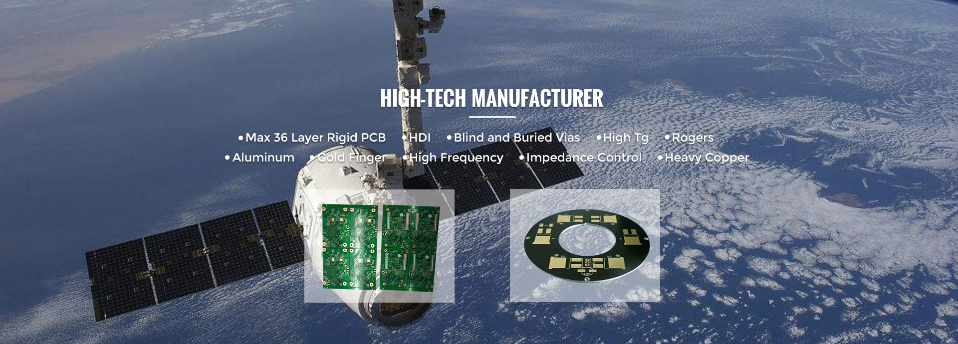
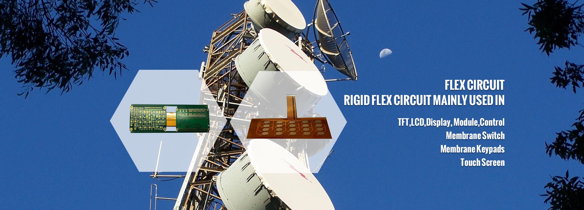
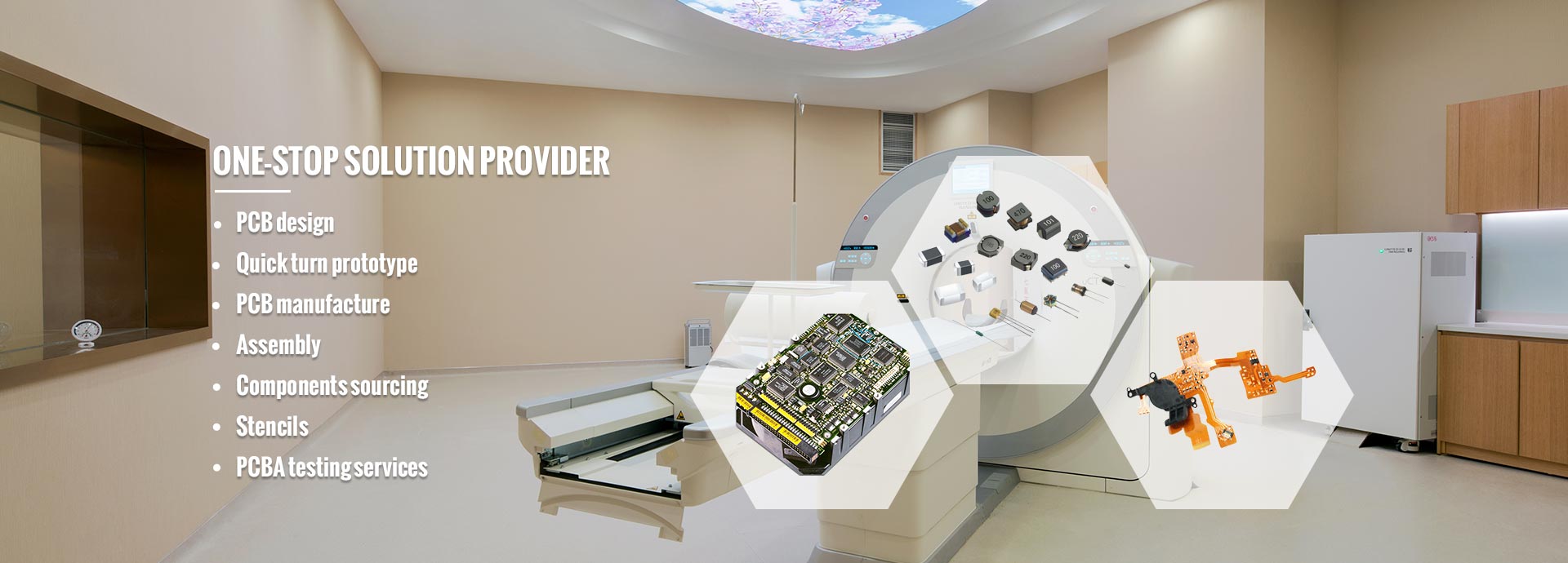
Dear Partners, welcome to MINKINZI – China’s Trusted End-to-End Manufacturing Partner, with 20 years of expertise, we specialize in: Design & Development → Max 58 Layer PCB Fabrication →Turnkey PCBA Assembly → Box-Build Assembly. ODM/OEM/Contract Manufacturing tailored to global standards. Support DFM. Welcome to send your NDA, PCB Gerber, BOM, so that we can provide quotation for you. .

  • Ventec VT-901 High-Tg Halogen-Free PCB Laminate | Superior Thermal Reliability

  • Ventec VT-901 High-Tg Halogen-Free PCB Laminate | Superior Thermal Reliability

  • Ventec VT-901 High-Tg Halogen-Free PCB Laminate | Superior Thermal Reliability

  • Ventec VT-901 High-Tg Halogen-Free PCB Laminate | Superior Thermal Reliability

  • Ventec VT-901 High-Tg Halogen-Free PCB Laminate | Superior Thermal Reliability

Ventec VT-901 High-Tg Halogen-Free PCB Laminate | Superior Thermal Reliability

PCB Layer:24    PCB Application:Automotive

/Industrial/Communications

We have Ventec VT-901 Series material

 in stock.

Include but not limited to the below:

VT-4A2HPVT-46VT-890
VT-4B5VT-5AVT-901
VT-4BCVT-5A2VT-90
VT-4A2HVT-441VT-90H
VT-42BVT-447VT-3C
VT-47VT-481VT-5CC
VT-3AVT-870VT-TL
VT-4AVT-871VT-MC
VT-4A2VT-880VT-Heat


Share

Description :

Minkinzi: Ventec VT-901 PCB: Comprehensive Overview, Technical Characteristics, and Industry Applications

I. Overview of Ventec VT-901 PCB Material

Ventec VT-901 is a high-performance PCB substrate material manufactured by Ventec Electronics, belonging to a high-frequency and high-speed material system based on modified epoxy resin with a specialized formulation. Engineered to deliver exceptional electrical performance, thermal stability, and mechanical reliability, VT-901 has become a trusted choice across demanding industries such as automotive electronics, 5G communications, industrial control, and aerospace. Its balanced combination of low signal loss, robust thermal endurance, and processability makes it a versatile solution for both VT-901 RF PCB and VT-901 high-speed digital PCB designs, as well as mission-critical applications requiring long-term reliability.


II. Key Characteristics of Ventec VT-901 PCB

PropertySpecification
Glass Transition Temperature (Tg)≥ 150°C (High-Tg system)
Dielectric Constant (Dk)Low-loss design; suitable for high-frequency signal transmission
Dissipation Factor (Df)Extremely low dielectric loss; excellent signal integrity
Decomposition Temperature (Td)≥ 340°C
CTE (Coefficient of Thermal Expansion)Low Z-axis CTE; enhances PTH reliability
Water AbsorptionLow water absorption; high hygrothermal stability
Flammability RatingUL94 V-0
Process CompatibilityCompatible with lead-free soldering; RoHS/REACH compliant

These specifications make Ventec VT-901 particularly well suited for high-frequency laminate applications including VT-901 microwave PCB designs, where signal attenuation and phase stability are critical performance parameters. The material's stable Dk across frequency and temperature ranges also supports precision impedance control for both analog RF front ends and high-speed digital backplanes.


III. Main Application Areas for Ventec VT-901 PCB

The versatility of Ventec VT-901 enables its deployment across a broad spectrum of industries and end-use scenarios. Whether your project demands high-frequency signal transmission, high reliability in harsh environments, or robust power handling, VT-901 delivers consistent performance.

5G Communication and Telecom Infrastructure VT-901 is widely adopted in 5G base stations, antenna systems, and RF front-end modules, where its low Df and stable Dk ensure minimal signal loss and superior signal integrity. As a leading VT-901 telecom PCB material, it supports the high data rate and low latency requirements of next-generation wireless networks, including massive MIMO antennas, millimeter-wave transceivers, and small-cell base stations.

Automotive Electronics and ADAS The material meets AEC-Q automotive qualification standards, making it ideal for advanced driver-assistance systems (ADAS), automotive radar (24 GHz / 77 GHz), engine control units (ECUs), and electric vehicle power electronics. Automotive radar modules built on VT-901 deliver stable dielectric performance across wide temperature ranges, ensuring accurate object detection and reliable operation in safety-critical applications.

Defense and Military-Grade Electronics For mission-critical applications requiring the highest levels of reliability, VT-901 stands as a proven VT-901 military grade PCB solution. It is deployed in electronic warfare systems, radar platforms, secure communication equipment, and avionics where performance under extreme thermal, mechanical, and environmental stress is non-negotiable. Its compatibility with hermetic packaging and ruggedized assembly processes further reinforces its defense credentials, making it a strong VT-901 defense PCB choice for military contractors and aerospace system integrators.

Industrial Controls and Power Electronics VT-901's high heat resistance and excellent mechanical impact resistance make it suitable for industrial automation, motor drives, power conversion modules, and high-power LED lighting systems. For high-current, high-voltage applications, the material's thermal robustness and low Z-axis CTE support reliable plated-through-hole connections, positioning it as a dependable VT-901 power electronics PCB substrate for converters, inverters, and industrial power modules.

Aerospace and Avionics The material's reliability in harsh environments — including extreme temperatures, vibration, and humidity — makes it well-suited for aerospace and military equipment. Flight control systems, satellite communication payloads, and avionics display modules benefit from VT-901's stable electrical and mechanical properties over extended service lifetimes.

High-Speed Servers and Data Centers Modern data center infrastructure demands materials that preserve signal integrity at multi-gigabit data rates. As a high-performance VT-901 data center PCB material, it supports high-speed backplanes, network switches, server motherboards, and storage systems where maintaining tight impedance tolerances and minimizing insertion loss are essential. Its excellent Dk stability also enables the design of VT-901 high-speed digital PCB architectures for next-generation computing platforms.

LED Lighting and High-Power Illumination VT-901's excellent thermal dissipation performance and high Tg make it an ideal substrate for high-power LED lighting applications, where heat management directly impacts lumen maintenance and product lifespan.

Medical Electronic Equipment For medical applications requiring high reliability and long-term stability, VT-901 serves as a certified-grade VT-901 medical device PCB material. It is used in patient monitoring systems, diagnostic imaging equipment, portable medical devices, and laboratory instruments where signal clarity, biocompatibility compliance, and consistent performance are essential.

IoT and Edge Computing Devices As the Internet of Things expands into industrial, consumer, and smart city applications, VT-901 emerges as a reliable VT-901 IoT PCB substrate. Its combination of low signal loss, compact form-factor support, and robust environmental performance enables wireless sensor nodes, edge gateways, smart home hubs, and connected industrial devices to operate reliably across diverse deployment scenarios.


IV. Ventec VT-901 Processing Highlights

Successful fabrication of Ventec VT-901 PCBs requires careful control of each manufacturing stage. The following processing recommendations ensure optimal electrical performance, mechanical integrity, and long-term reliability.

Lamination Process A vacuum press lamination process is recommended to ensure robust interlayer bond strength and minimize voids. Proper cure profiles and ramp rates are essential to achieve full resin polymerization, particularly in multilayer stack-ups used in VT-901 microwave PCB and VT-901 high-speed digital PCB designs.

Drilling Parameters Drilling parameters must be optimized for the material's Tg range to avoid rough hole walls, smear, or delamination. Controlled entry and exit speeds, appropriate drill bit types, and desmearing processes help maintain clean hole walls for reliable plating.

Plating and Copper Deposition PTH (Plated-Through-Hole) reliability must be ensured through proper electroless copper deposition, electrolytic plating, and thermal stress testing. The low Z-axis CTE of VT-901 contributes to excellent PTH performance under lead-free reflow conditions.

Surface Finish Compatibility VT-901 is compatible with a wide range of surface finishes, including ENIG (Electroless Nickel Immersion Gold), OSP (Organic Solderability Preservative), Immersion Silver, Immersion Tin, and HASL (Hot Air Solder Leveling), providing flexibility for various assembly requirements.

Impedance Control Strict control of impedance tolerance (±10% or better) is required for high-frequency applications. Tightly managed dielectric thickness, copper weight uniformity, and stack-up symmetry are essential to meet signal integrity specifications, particularly in VT-901 RF PCB and VT-901 telecom PCB designs.


V. How to Select a Manufacturer for Ventec VT-901 PCB

Choosing the right manufacturing partner is critical to realizing the full performance potential of Ventec VT-901. Whether you require a PCB fabricator, an EMS provider, or a turnkey PCBA solution, the following guidance will help you make an informed decision.

Selecting a PCB Manufacturer (Fabricator)

Key Considerations:

✅ Material Certification: UL certification and demonstrated production experience with Ventec materials ensures the manufacturer understands VT-901's processing nuances.

✅ Layer Count Capability: The ability to manufacture high-layer-count boards (from 2 layers to 30+ layers) supports everything from simple single-layer designs to complex multilayer backplanes used in VT-901 data center PCB and VT-901 defense PCB applications.

✅ High-Frequency Processes: Capabilities such as impedance control, back-drilling, and buried/blind vias are essential for high-speed and high-frequency designs.

✅ Quality Systems: Compliance with ISO 9001, IATF 16949 (automotive grade), and AS9100 (aerospace) certifications demonstrates a commitment to industry-recognized quality standards.

✅ Equipment Configuration: Modern equipment including vacuum presses, LDI (Laser Direct Imaging) exposure machines, AOI (Automated Optical Inspection), X-Ray, and flying probe testers ensures precision manufacturing and thorough inspection.

✅ Lead Time & Capacity: The ability to meet needs ranging from small-batch prototyping to high-volume mass production provides scalability as your project grows.

 Selecting an EMS (Electronics Manufacturing Services) Provider

Key Considerations:

✅ Assembly Processes: SMT line configuration with placement accuracy of ±0.03mm ensures precise component mounting, even for fine-pitch packages.

✅ BGA/QFN Capabilities: Support for package sizes down to 01005, including fine-pitch BGAs and QFNs, enables high-density designs.

✅ AOI/X-Ray Inspection: 3D X-Ray inspection capability for BGA solder joint quality verification is critical for high-reliability applications such as VT-901 medical device PCB and VT-901 military grade PCB assemblies.

✅ Testing Capabilities: Comprehensive testing including ICT (In-Circuit Test), FCT (Functional Circuit Test), flying probe testing, and burn-in testing ensures product reliability.

✅ Certifications: ISO 13485 (medical), IATF 16949 (automotive), and IPC-A-610 compliance demonstrate adherence to industry-specific quality requirements.

✅ Supply Chain Management: Robust component sourcing channels, alternative part solutions, and BOM optimization capabilities help mitigate supply chain risks.

Selecting a Turnkey/PCBA Provider (One-Stop Service)

Key Considerations:

✅ Component Authenticity: Authorized manufacturer channels and full component traceability protect against counterfeit parts, which is especially critical for VT-901 defense PCB and VT-901 military grade PCB applications.

✅ BOM Sourcing Capability: Status as an authorized distributor ensures genuine components and competitive pricing.

✅ DFM Optimization: Design for Manufacturability analysis prior to production identifies potential issues early, reducing costly rework and time-to-market delays.

✅ Cost Optimization: Recommendations for alternative parts and bulk purchasing advantages help reduce overall BOM cost without compromising quality.

✅ Lead Time Assurance: End-to-end cycle management from order placement to delivery provides predictability and reliability.

✅ One-Stop Service: Integrated delivery covering PCB fabrication, component sourcing, SMT assembly, testing, and packaging simplifies project management and reduces coordination overhead.

Comprehensive Recommendations for Selecting a Contract Manufacturer

Evaluation CriteriaKey Considerations
Technical CompatibilityDocumented experience processing Ventec VT-901; review of past projects and customer references
Quality ManagementAdherence to IPC standards; implementation of full traceability systems
ResponsivenessSpeed of quoting, engineering communication efficiency, and issue resolution capability
Cost TransparencyClear quote structure with no hidden fees; detailed cost breakdown
ConfidentialityNDA signing to protect client design data and intellectual property
After-sales ServiceResponsive complaint handling, rework services, and ongoing technical support

VI. Core Advantages of the Minkinzi Factory

Why Choose Minkinzi as Your Ventec VT-901 Partner?

Extensive Ventec Material Processing Experience Minkinzi brings proven expertise in key VT-901 processes including lamination, drilling, and plating. Our engineering team understands the nuances of working with this advanced material and consistently delivers high-quality results for applications ranging from VT-901 IoT PCB prototypes to VT-901 power electronics PCB production runs.

One-Stop PCBA Services We provide comprehensive solutions covering PCB fabrication, component sourcing, SMT assembly, and final testing. This integrated approach simplifies your supply chain, reduces lead times, and ensures seamless coordination across all production stages.

Professional Engineering Team Our value-added services include DFM (Design for Manufacturability) checks, impedance simulation, and BOM optimization. Whether your design is a VT-901 RF PCB for wireless communications or a VT-901 high-speed digital PCB for data center infrastructure, our engineers work alongside you to optimize manufacturability and performance.

Strict Quality Control Full compliance with IPC-A-610 and IATF 16949 standards ensures that every board leaving our facility meets the highest quality benchmarks. Our quality management system is designed to support the stringent requirements of automotive, medical, and defense applications.

Flexible Production Models We support everything from small-batch prototyping to large-scale mass production, providing the flexibility needed to scale your project from initial concept through full production ramp.

Trusted by Global Clients Minkinzi serves customers across Europe, the Americas, Southeast Asia, the Middle East, and beyond. Our international experience enables us to understand and meet the diverse regulatory, logistical, and technical requirements of global markets.

Rapid Quote Response Professional quotations are provided within 24 hours, enabling you to make fast, informed decisions and keep your project timelines on track.

Confidentiality and Security We strictly adhere to NDAs to safeguard your intellectual property and design data. Our information security protocols ensure that sensitive project information remains protected throughout the engagement.


Welcome to contact the Minkinzi factory for Ventec VT-901 PCB manufacturing: Email: sales@minkinzi.com

Applications :

entec VT-901 PCB Manufacturing Solutions — Showcasing Minkinzi's Capabilities for High-End Clients

Discover the Power of Ventec VT-901: Premium High-Frequency PCB Material

What Is Ventec VT-901?

Ventec VT-901 is a premium high-frequency, high-speed copper-clad laminate (CCL) engineered by Ventec Electronics. As a flagship product within the VT-901 / VT-90H series, this advanced VT-901 high-Tg laminate is purpose-built for mission-critical applications that demand ultra-low signal loss, exceptional thermal reliability, and uncompromising signal integrity.

Engineered as a true VT-901 low Dk / low Df material, VT-901 delivers industry-leading electrical performance:

  • Extremely low dissipation factor (Df): approximately 0.0035–0.005 at 10 GHz — far superior to standard FR-4, making it an ideal VT-901 low-loss PCB solution.

  • High decomposition temperature (Td): ≥ 390°C, allowing the material to withstand multiple reflow cycles and severe thermal shock processes — a defining characteristic of VT-901 high thermal performance.

  • Low and stable coefficient of thermal expansion (CTE): Excellent Z-axis CTE, perfectly suited for high-layer-count, high-reliability PCB stack-ups.

  • Lead-free process compatibility: Fully compliant with IPC-4101 high-Tg requirements, qualifying it as a dependable VT-901 lead-free PCB material.

  • Halogen-free formulation: Designed as a VT-901 halogen-free laminate to meet global environmental and safety standards.

  • Full UL certification: 94 V-0 flame retardancy rating for maximum safety assurance.

Where Ventec VT-901 Excels: Typical Application Areas

Application AreaCustomer TypeCore Requirements
5G Base Stations / Antenna ModulesTelecom Equipment ManufacturersLow loss, high-frequency signal integrity
Data Center Switches / RoutersNetwork Equipment Manufacturers56 Gbps+ high-speed signal transmission
Optical Modules (100G / 400G / 800G)Optical Communication ManufacturersHigh frequency, stable low Dk / Df
Automotive ADAS / Millimeter-wave RadarTier 1 Component SuppliersHigh heat resistance, reliability, AEC-Q100 compatibility
Aerospace / Satellite CommunicationDefense & Research InstitutesExtreme environment resistance, lightweight
Industrial Control / High-end Power SuppliesIndustrial Equipment ManufacturersHigh-voltage insulation, thermal management
AI Accelerator Cards / ServersComputing Hardware ManufacturersHigh-speed serial transmission, thermal reliability

Overcoming the Complex Challenges of VT-901 PCB Fabrication

Working with a high-performance substrate like Ventec VT-901 requires specialized expertise, advanced equipment, and tightly controlled processes. At Minkinzi, we have refined our manufacturing workflow to consistently deliver VT-901 high reliability PCB solutions that exceed the expectations of the world's most demanding industries.

Material Storage and Pre-Treatment

VT-901's high-Tg resin system and specialized chemistry make the laminate highly sensitive to humidity. Any absorbed moisture can cause white spots, measling, or delamination during the lamination cycle.

Our Solution: We store all VT-901 materials in a climate-controlled environment (temperature 20 ± 5°C, humidity ≤ 30% RH) and bake each panel at 120°C for 4–8 hours prior to production. This meticulous pre-treatment safeguards against moisture-driven defects and preserves the integrity of the VT-901 signal integrity and VT-901 power integrity performance.

Drilling Process Challenges

The unique resin system of VT-901 can lead to rough hole walls, nail-heading, and glass fiber pull-out during mechanical drilling — risks that become amplified in backplanes and high-layer-count designs.

Our Solution:

  • Premium carbide drill bits sourced from Union Tool (Japan) or Drill-Ba.

  • Strict stack height control (≤ 3 panels) to ensure consistent hole quality.

  • Optimized drilling parameters: infeed speed ≤ 80 IPM with retraction speed increased by 30%.

  • Achieved hole wall roughness Ra ≤ 1.5 μm, far exceeding IPC-6012 Class 3 standards — a critical benchmark for any VT-901 high reliability PCB.

Hole Metallization and Plating

Low-Df resin systems typically exhibit weak chemical affinity, which can compromise copper-to-hole-wall adhesion and lead to voids, plating delamination, or other latent reliability issues. This is especially problematic when designing VT-901 CAF resistant PCB structures for long-term field deployment.

Our Solution:

  • Plasma treatment combined with a modified Black Hole or brown oxide process (with plasma pre-treatment when not using traditional colloidal palladium).

  • Vertical Continuous Plating (VCP) line ensuring plating uniformity ≥ 90%.

  • Multiple backlight inspection steps; hole copper thickness ≥ 25 μm, comfortably meeting 1 oz board requirements.

Lamination Process

High-Tg materials like VT-901 exhibit low resin flow, which can cause resin starvation, layer misalignment, and poor inner-layer copper-to-dielectric adhesion if not properly managed.

Our Solution:

  • Vacuum laminator operating at ≤ 50 mTorr for void-free bonding.

  • Low-ramp-rate lamination profile (1.5°C/min) to optimize resin flow and cure behavior.

  • Symmetrical stack-up design to balance thermal expansion across the entire PCB — essential for maintaining VT-901 power integrity in dense, high-current designs.

Impedance Control — The Heart of VT-901 Signal Integrity

Although VT-901 offers a stable Dk, many customers require tight impedance tolerances of ±5% or even ±3% to guarantee flawless VT-901 signal integrity at multi-gigabit data rates.

Our Solution:

  • Closed-loop process combining Polar Si8000 / Si9000 impedance calculation with TDR measurement verification.

  • Trace width / spacing capability down to 3 mil / 3 mil (76 μm) for mass production.

  • Standard impedance tolerance of ±5%, with high-end capability of ±3% for the most demanding RF and high-speed digital applications.

Surface Finish Compatibility

The low-roughness copper foils commonly paired with VT-901 (such as VLP, RTF, and HVLP2) can present adhesion challenges with certain surface finishes.

Our Solution:

  • Proven compatibility with HVLP3 low-roughness copper foil (Ra ≤ 0.5 μm).

  • Full compatibility across ENIG, Immersion Silver, OSP, and lead-free HASL finishes — ensuring every VT-901 lead-free PCB material stack-up can be finished to customer specification.

High-Layer-Count Boards and Back-Drilling

Customer designs frequently call for 12 to 20+ layers with back-drilled vias, and stub lengths must be controlled to within 8 mils to preserve signal performance.

Our Solution:

  • 6-axis CNC controlled-depth back-drilling with depth tolerance of ±2 mils.

  • Stacking accuracy of ±0.15 mm, achieved through a high-precision positioning system.


Rigorous Quality Control That High-End Clients Demand

Minkinzi operates under a comprehensive quality management framework designed to satisfy the most exacting OEM and Tier 1 supplier requirements. Every VT-901 high reliability PCB we ship is backed by full documentation, traceability, and validated process control.

Certified Quality Management Systems

  • IATF 16949 (Automotive)

  • ISO 9001 / ISO 14001 / ISO 45001 Integrated Management System

  • UL Certification

  • AS9100D (Aerospace & Defense)

  • IPC-A-600 / IPC-6012 Class 3

Material Management Excellence

  • Sourced directly from Ventec or Tier-1 authorized distributors, with Certificate of Conformance (CoC) provided for every batch.

  • Incoming material inspection includes spot checks on Tg, Dk / Df, CTE, and water absorption — confirming the VT-901 halogen-free laminate and electrical properties meet datasheet specifications.

  • Re-inspection cycle shortened by 20% beyond standard specifications for added confidence.

In-Process Control and Inspection

Control PointOur Capabilities
AOI8-axis high-definition AOI; missed defect rate < 0.01% for 0.3 mm pitch ICs
X-RAYHitachi X-ray; 100% inspection for blind vias, back-drilling, and BGAs
Impedance TestPolar CITS900s with TDR full-board scanning
Cross-section / MetallographyIn-house laboratory; report issued within 48 hours
Flying Probe / Universal TestTDK flying probe tester; 100% open / short circuit testing
Thermal Shock / Stress288°C for 10s, 3 cycles; no measling or delamination

Reliability Testing Capabilities

Our in-house laboratory is equipped to execute the full suite of reliability tests per IPC-TM-650 standards, including:

  • IST (Interconnect Stress Test)

  • SIR (Surface Insulation Resistance)

  • TCT (Temperature Cycling)

  • HTSL / HTST (High-Temperature Storage Life / Test)

These capabilities are vital for validating VT-901 CAF resistant PCB performance over the product lifecycle.

Full Documentation and Traceability

  • MES full-process traceability system: every board carries a unique QR code.

  • Real-time online production progress tracking for customer visibility.

  • Strict data confidentiality: NDA signing, dedicated secure workshop, and encrypted file transfer.


Flexible Delivery Capabilities Designed Around Your Project

Delivery Commitments

Layer Count / TypeStandard Lead TimeRush Order Response
4–8 Layer Prototypes5–7 days24h expedited service
10–16 Layer Prototypes7–10 days3-day expedited service
18+ Layers10–15 daysProject-specific assessment
Small Batch (≤ 50 m²)12–15 daysNegotiable
Medium Batch15–20 daysProject-specific assessment

Production Capacity and Flexibility

  • Monthly capacity exceeding 30,000 m².

  • Full-stage support: prototype → small batch → medium batch → large-scale production.

  • Dedicated rush order channel: 48-hour quote response and dedicated engineer support via group chat.

Global Logistics Network

  • Direct shipping via SF Express, DHL, FedEx, and UPS — 3 to 5 day door-to-door delivery worldwide.

  • Flexible trade terms including DDP and DAP.

  • Overseas warehouses and agents in the USA and Germany for faster regional fulfillment.

Built-In Risk Mitigation

  • Dual-supplier backup for critical materials to safeguard against Ventec stock shortages.

  • Primary and backup production lines, plus off-site facilities, to eliminate single-point-of-failure risks.

  • Capacity reservation agreements (SLA) available for major ongoing orders.


Partner with Minkinzi for Your Next Ventec VT-901 PCB Project

When your application demands a VT-901 low-loss PCB with flawless VT-901 signal integrity and proven VT-901 high thermal performance, Minkinzi delivers the engineering depth, process discipline, and global service infrastructure to bring your most ambitious designs to life. Whether you are developing 5G infrastructure, next-generation AI servers, automotive radar, or aerospace communication systems, our team is ready to support you from prototype through mass production.

Contact Minkinzi today to start your Ventec VT-901 PCB project: Email: sales@minkinzi.com

Flow Chart :

Minkinzi: Ventec VT-901 High-Frequency PCB Material—From Samples to Mass Production

One-stop engineering services to accelerate the deployment of high-end applications including 5G, automotive radar, and satellite communications.


About Ventec VT-901 PCB

The Ventec VT-901 PCB is a high-performance, PTFE-based copper clad laminate engineered specifically for high-frequency, high-speed applications. With a low-loss, ceramic-filled formulation, this Ventec VT-901 laminate delivers outstanding stability in dielectric constant (Dk) and dissipation factor (Df), making it a foundational material in advanced electronic systems such as 5G infrastructure, millimeter-wave radar, satellite communications, and aerospace platforms.

As a trusted VT-901 PCB material choice for RF engineers worldwide, the Ventec VT-901 substrate has earned its reputation for reliability in the most demanding signal-integrity environments. Whether you require a VT-901 high frequency PCB for mass deployment or a custom Ventec VT-901 PCB board for prototyping, this laminate family offers a scalable, production-ready solution.

Key Features at a Glance

ParametersPerformance Indicators
Dielectric Constant (Dk)3.0–3.5 (10 GHz)
Loss Factor (Df)0.0025–0.0035 (10 GHz)
Glass Transition Temperature (Tg)>280°C
Coefficient of Thermal Expansion (CTE)Extremely low, excellent dimensional stability
Temperature Coefficient of Dielectric Constant±0.05 ppm/°C (Excellent)
Frequency CoverageDC ~ 77 GHz+

The Complete Process: From Sample to Mass Production for VT-901 PCB Laminate

Requirements Assessment and Material Selection

Every successful build begins with a thorough evaluation. Our team works directly with you to define frequency targets, layer count, impedance requirements, reliability class, and end-use environment. Our FAE (Field Application Engineering) team then recommends the optimal Dk/Df, thickness, and copper-foil combination for your Ventec VT-901 PCB board design.

We also assess the compatibility of multiple Ventec VT-901 laminate grades—including VT-901, VT-901S, and VT-901H—to ensure the selected VT-901 PCB laminate precisely matches your application's electrical, thermal, and mechanical requirements.

Deliverable: A formal Material Selection Recommendation paired with a Preliminary DFM (Design for Manufacturability) assessment.

Our Value: As an officially authorized Ventec partner, Minkinzi has direct access to the latest Ventec VT-901 substrate specifications and a comprehensive failure-case database—dramatically shortening the material selection cycle for your project.


Engineering Document Confirmation and Quotation

Once the VT-901 PCB material is selected, your Gerber or ODB++ files are imported into our CAM system for full engineering review. Our engineers develop a tailored impedance-control strategy covering microstrip lines, striplines, and coplanar waveguides, and design the laminated stack-up for 8-layer, 12-layer, and multi-core board configurations.

Deliverable: A detailed Engineering Assessment Report and formal quotation. All critical parameters—trace width, spacing, dielectric thickness, copper weight—are locked at this stage to eliminate costly revisions later in the cycle.


Sample Preparation

Prototype fabrication of your Ventec VT-901 PCB follows tightly controlled process steps:

  • Material Pretreatment: PTFE-based VT-901 PCB laminate requires a special baking cycle (150°C × 2h) to eliminate absorbed moisture before lamination.

  • Drilling: Carbide drill bits paired with high-speed parameters prevent rough hole walls and ensure clean via formation.

  • Hole Metallization: Plasma treatment combined with chemical copper deposition guarantees strong hole-wall adhesion and reliable via conductivity.

  • Lamination: High-temperature, high-pressure lamination (>200°C, >300 PSI) using specialized buffer materials ensures void-free bonding across every layer of the Ventec VT-901 PCB board.

  • Surface Treatment: Immersion nickel gold (ENIG), immersion silver, or OSP finishes are available based on your assembly and reliability needs.

Sample Delivery: 5–25 pieces with rapid turnaround.

Shipment Inspection Report Includes: Impedance measurements, IST/TCT reliability data, and cross-section metallographic analysis.


Testing, Verification, and Certification Support

Once samples reach your facility, our team supports a full validation cycle:

  • Electrical Performance: S-parameters, insertion loss, and return loss verification on your VT-901 high frequency PCB prototypes.

  • Thermal Reliability: Thermal cycling from -55°C to +125°C for 1,000 cycles to confirm long-term stability of the Ventec VT-901 copper clad laminate.

  • Long-Term Aging: 85°C / 85% RH humidity aging test.

  • Industry Certifications: UL listing and IPC-6012 Class 3 / 3A compliance.

Minkinzi Provides:

  • Cross-section analysis and metallographic reporting

  • TDR (Time Domain Reflectometry) impedance testing

  • Failure analysis support through our in-house FA Lab


Small-Batch Pilot Production

Before committing to full-volume manufacturing, a controlled pilot run confirms process stability for the Ventec VT-901 laminate in your design.

  • Volume Range: 30–100 pieces

  • Yield Target: ≥95%

  • Process Calibration: Drilling, copper plating, lamination, and etching parameters fully solidified

  • Deliverable: Complete PPAP/APQP documentation package, including SPC control charts, PFMEA, and process flow diagrams

This stage ensures your Ventec VT901 PCB transitions seamlessly from prototype to scalable production.


Mass Production

When your VT-901 PCB design is locked and validated, we move into full mass-production mode with rigorous quality governance:

  • Production Scheduling: Real-time WIP (Work-In-Process) tracking with full traceability from raw material to finished board

  • Process Quality Control: AOI inspection, impedance testing, and plating thickness monitoring at every critical stage

  • 100% Online Testing: Key processes verified for every VT-901 PCB material panel

  • Packaging: Vacuum packaging, moisture-proof bags, and desiccant included—fully compliant with MSD (Moisture Sensitive Device) handling standards

Capacity and Lead Time:

  • Standard lead time: 10–15 working days

  • Expedited service: 7 working days (subject to engineering evaluation)

  • Monthly capacity: Over 30,000 sqft of high-frequency boards


Shipment and After-Sales Service

Your project doesn't end at delivery—it evolves through our lifetime support model:

  • Complete COQ (Cost of Quality) Report included with every shipment

  • Dedicated 1-on-1 Project Manager for lifetime follow-up

  • On-Site Technical Support including VAVE (Value Analysis / Value Engineering) and cost-reduction recommendations

  • 8D Problem-Solving Report delivered within 24 hours of any issue


Why Choose Minkinzi for Your Ventec VT-901 PCB

DimensionsOur Advantages
Material LicensingVentec Strategic Partner with direct supply from the original manufacturer of the Ventec VT-901 copper clad laminate
Process ExperienceOver 200 VT-901 PCB projects delivered, spanning 5G AAU, 77 GHz automotive radar, and LEO satellite payloads
Testing CapabilitiesFull suite of high-frequency test equipment including a 110 GHz Vector Network Analyzer, TDR, and IST systems
Delivery GuaranteeSamples in as fast as 7 days; batch production in 10–15 days
Cost AdvantageGroup-wide material procurement combined with intelligent scheduling reduces single-board cost by 8–15%

When you choose Minkinzi, you're choosing a partner that understands the Ventec VT-901 substrate inside and out—and has the production pedigree to prove it.


Application Scenarios

The VT-901 high frequency PCB is the material of choice across a broad range of mission-critical applications:

  • 5G Communication Base Stations (AAU / RRU)

  • 77 GHz Millimeter-Wave Automotive Radar

  • LEO Satellite Communication (Ku / Ka Band)

  • Aerospace Phased Array Radar

  • Medical Imaging Systems

  • Test and Measurement Instruments

From prototype to mass production, the Ventec VT-901 PCB board continues to enable the next generation of wireless innovation.


Start Your Ventec VT-901 PCB Project Today

Minkinzi offers a free DFM assessment and 24/7 quotation response to accelerate your path from sample to mass production.

Whether you need a single prototype VT-901 PCB laminate panel or full-scale volume manufacturing of the Ventec VT901 PCB, our engineering and production teams are ready to support your most demanding high-frequency designs.

Contact Minkinzi today to manufacture your Ventec VT-901 PCB with confidence. Email: sales@minkinzi.com

Capability :

One-Stop Manufacturing Service (PCB/PCBA) for Ventec VT-901 High-Frequency, High-Speed Materials

Premium High Tg Ventec VT-901 PCB Manufacturing | Low Loss & High-Speed Solutions from Minkinzi

When your design demands uncompromising signal integrity, thermal stability, and long-term reliability, Minkinzi's one-stop PCB and PCBA turnkey service for Ventec VT-901 delivers the precision your high-frequency and high-speed applications require. As a Ventec Tier-1 strategic partner, we combine deep materials expertise with advanced manufacturing capabilities to produce low loss VT-901 PCB solutions trusted by Tier-1 automotive suppliers, 5G infrastructure leaders, aerospace integrators, and AI server innovators worldwide.


Why Ventec VT-901 Is the Industry's Go-To High Frequency VT-901 Laminate

Ventec VT-901 is a ceramic-filled hydrocarbon high frequency VT-901 laminate engineered for next-generation mmWave and high-speed digital systems. Its balanced electrical, thermal, and mechanical performance makes it a preferred substrate for designers who refuse to compromise.

Key Material Properties:

  • Low Df VT-901 PCB performance: Dissipation factor (Df) ≤ 0.0025 at 10 GHz for ultra-low insertion loss

  • Low Dk VT-901 PCB behavior: Stable dielectric constant (Dk 3.0–3.5) with minimal variation across frequency and temperature

  • High Tg Ventec VT-901 PCB reliability: Glass transition temperature ≥ 150°C, fully qualified for lead-free assembly including 260°C reflow soldering

  • Thermally resistant VT-901 PCB design: Thermal conductivity of 0.42 W/m·K for excellent heat dissipation under high power density

  • Halogen-free VT-901 PCB compliance: RoHS-aligned chemistry meeting strict environmental and safety standards

  • Lead-free VT-901 PCB assembly compatibility: Full FR-4 process compatibility for drilling, lamination, and copper deposition

  • High reliability VT-901 PCB construction: Excellent CAF resistance and proven long-term reliability under thermal and humidity stress

Typical High-Speed VT-901 PCB Applications:

  • 5G base stations and active antenna units (AAU)

  • 77 GHz automotive millimeter-wave radar

  • Satellite communications and LEO payload electronics

  • AESA phased-array radar and defense systems

  • Aerospace avionics and guidance systems

  • Test & measurement instrumentation

  • AI servers, 800G switches, and high-end networking backplanes


Minkinzi Factory Positioning: Your Specialist in High Frequency and High-Speed PCB Manufacturing

Minkinzi specializes in high-end PCB fabrication and one-stop PCBA turnkey services with deep expertise in high-frequency materials including VT-901, RO4350B, RO4003C, RT/duroid 5880, TLX, and TLY, as well as high-speed mixed-material (hybrid) stack-up structures. Our engineering team understands the nuances of low-loss material processing, controlled impedance routing, and mmWave signal integrity — translating your Gerber files into boards that meet the most demanding electrical and mechanical specifications.

Comprehensive Manufacturing Capabilities

CapabilitySpecification
Layer Count2 – 30 layers, including 4–12 layer mixed lamination
Board Thickness0.2 mm – 3.2 mm
Min. Line Width/Spacing3 mil / 3 mil (75 μm)
Min. Hole Diameter4 mil (0.10 mm) mechanical; 2 mil laser drill
Aspect RatioUp to 12:1
Copper ThicknessInner: 1/3 oz – 2 oz; Outer: 1 oz – 6 oz
Surface FinishENIG, ENEPIG, Immersion Silver, Immersion Tin, OSP, Gold Plating, Hard Gold Plating
Impedance Control±5% (50Ω, 90Ω differential, coplanar waveguide supported)
Special ProcessesStepped slots, depth-controlled drilling, back-drilling, buried/blind vias, HDI (Any-layer), Rigid-flex PCBs

Expertise in High-Frequency Material Processing

Our factory is purpose-built for low-loss and mixed-dielectric PCB production, including:

  • VT-901 Mixed Lamination: VT-901 + FR-4, VT-901 + 370HR, and VT-901 + VT-47 hybrid stack-ups that use different dielectric constants in different board zones to optimize cost and performance

  • Low-Roughness Copper Foil Processing: HVLP3 / HVLP4 copper foil lamination for stable insertion loss in the mmWave frequency band

  • High-Precision Lamination: Narrow temperature and pressure control windows validated by CAE simulation combined with physical TMA measurement

  • Laser Trimming / Laser Profiling: Minimizing CNC-induced stress that can otherwise alter material electrical properties

Full-Service PCBA Capabilities

  • SMT Assembly: 01005 / 0201 components, BGA, CSP, QFN, PoP, with minimum pitch down to 0.25 mm

  • Full-Process Inspection: AOI, X-Ray, 3D SPI, ICT, and FCT for zero-defect delivery

  • Conformal Coating, Potting, and Underfill: For harsh-environment and high-reliability products

  • BGA Rework and Re-balling: Recovery services for engineering prototypes and low-volume builds

  • Supply Chain Support: BOM kitting, alternative component recommendations, and long-term material inventory management


Production Capacity Built for Prototyping and Scale

  • Monthly PCB Capacity: 35,000 m², including 8,000 m² dedicated to high-frequency boards

  • Monthly PCBA Capacity: 12 million placement points across 4 SMT lines, 3 post-soldering lines, and 2 conformal coating lines

  • VT-901 Dedicated Line Capacity: 3,000 m² per month — equally suited to small-batch prototyping and medium-volume mass production

  • Response Time: Prototyping in as little as 5 working days (including material preparation); 48-hour expedited service available for urgent projects


Supply Chain Strength: Ventec Tier-1 Partnership and Turnkey Sourcing

As a Ventec Tier-1 distributor and strategic partner, Minkinzi secures stable supply of the full VT-901 series, including VT-901 prepreg, to insulate your project from market volatility.

  • BOM Component Sourcing: Deep partnerships with Arrow, Avnet, WPG, and Future Electronics, with 100% authorized original manufacturer channels

  • Turnkey Manufacturing Model: Customers provide only Gerber files, BOMs, and schematics — we handle both labor and materials end-to-end

  • Material Inventory: Standing stock of 200–500 sheets of VT-901, RO4000 series, and PTFE materials to compress lead times

  • Alternative Material Solutions: Side-by-side performance comparison reports for material swaps (e.g., VT-901 ↔ RO4350B ↔ EM-390) to support cost-engineering without sacrificing performance


Cost Advantages That Lower Your Total Landed Cost

AdvantageCustomer Benefit
First-pass yield ≥ 96%Low scrap rate reduces cost impact on unit price
Bulk material procurementQuarterly Ventec orders exceed 100,000 sheets, securing Tier-1 pricing
Waived engineering feesEngineering fees waived for monthly orders ≥ 30 m²; tiered discounts for orders ≥ 100 m²
Turnkey price locking1–3 month BOM price-locking service mitigates chip price-hike risk
Dual-currency quoting (USD/RMB)Supports FOB, CIF, and DDU terms with flexible trade options

Indicative Pricing Reference (VT-901, 4-layer, 1.0 mm, ENIG finish):

  • Prototyping (5 pcs): ¥1,800 – ¥2,500 / m²

  • Mass Production (100 m²): ¥1,200 – ¥1,500 / m²

Final pricing varies by impedance requirements, hole count, copper thickness, and mixed-lamination complexity. Request a tailored quote today.


Lead Time and Global Delivery Commitments

Order TypeStandard Lead TimeExpedited Lead Time
VT-901 Prototyping (≤ 5 m²)7 – 10 days5 days
Mass Production (5–100 m²)12 – 18 days8 – 10 days
Mixed-Lamination Boards (5–8 layers)15 – 20 days12 days
PCBA (Turnkey/Assembly)5 – 10 days after material kitting3-day expedited option

Delivery Methods: Full coverage via SF International, DHL, FedEx, and TNT; supports DDP and FOB (Shenzhen/Hong Kong); dual-track logistics available with direct shipment from PCB factory and from PCBA factory to your warehouse.

Delivery Commitment: On-time delivery rate ≥ 98%; 1% of the order value deducted for every day of delay per contract terms.


Quality Control: Certified, Traceable, and Verified

System Certifications

  • ISO 9001:2015 Quality Management System

  • IATF 16949:2016 (Automotive Electronics)

  • ISO 13485:2016 (Medical, optional)

  • AS9100D (Aerospace, optional)

  • UL Certification (File No. E####)

  • IPC-A-600 / IPC-6012 Class 3 / Class 3A (High Reliability)

Process Control

  • First Article Inspection (FAI): AS9102 or PPAP FAI reports provided for 100% of orders

  • SPC (Statistical Process Control): Real-time monitoring of trace width, copper thickness, hole positioning, and impedance

  • Material Traceability: Mill Certificates for every batch of VT-901 laminate retained for ≥ 5 years

  • Full Inspection Coverage: AOI, X-Ray, cross-sectioning, and flying probe testing

  • In-line Dk/Df Sampling: Verified using Keysight N1500A dielectric analyzer + resonant cavity method

Testing Capabilities

  • Impedance Testing: Polar CITS900s (4-wire method)

  • Flying Probe / Fixture Testing: 100,000 points per day

  • Reliability Testing: Thermal shock (-55°C to +150°C), IST (Interconnect Stress Test), SIR (Surface Insulation Resistance), TMA, DSC, TGA

  • High-Frequency Testing: Supports customer-provided VNA (Vector Network Analyzer) test fixtures


Proven Track Record: VT-901 Case Studies Across Industries

Case 1: European 77 GHz Automotive Millimeter-Wave Radar

Customer: Tier-1 automotive electronics manufacturer (NDA protected) Materials: VT-901 + RO4350B hybrid lamination (6 layers) Features: Min. trace width 75 μm, 0.15 mm blind vias, ENEPIG surface finish, board thickness 0.8 mm ± 0.05 mm Volume: 500 pcs pilot + 5,000 pcs/month mass production Result: Impedance tolerance ±3%, AEC-Q100 automotive-grade certification passed, 99.2% first-pass yield sustained over 18 months of mass production.

Case 2: 5G Base Station AAU RF Unit

Customer: Domestic telecommunications ODM giant Materials: VT-901 + S1000-2M hybrid lamination (8 layers) Features: Back-drilling with ±0.05 mm stub tolerance, 0.20 mm buried vias, HVLP3 copper foil Volume: 1,200 units/month Result: Insertion loss outperformed customer spec by 0.3 dB/inch; zero batch defects over 2 years of mass production.

Case 3: Phased Array Radar T/R Module

Customer: Defense research institute Materials: VT-901 single-material (4 layers) Features: 0.10 mm laser vias, 30 μ" hard gold plating on gold fingers, back-drilling to specified stub depth Volume: 200-unit pilot run Result: Compliant with GJB 362B military standards; passed X-ray, ultrasonic scanning, and C-SAM inspection.

Case 4: High-End Test Instruments (Oscilloscopes / Spectrum Analyzers)

Customer: North American instrumentation company Materials: VT-901 + Megtron 6 hybrid lamination (10 layers) Features: 40 GHz signal integrity, differential impedance 90 Ω ±5% Volume: 300 units per batch Result: Eye diagram margin 15% higher than customer requirement, verified via Keysight ADS simulation.

Case 5: LEO Satellite Communication Payload

Customer: Commercial satellite company Materials: VT-901 + TC350 (backup option) Features: Radiation-resistant material selection advice, -65°C to +125°C temperature cycling Result: Assisted customer with ITAR compliance documentation; board passed vacuum-thermal cycling tests.

Case 6: High-Frequency Board for Medical Endoscope

Customer: Japanese medical device company Materials: VT-901 (4 layers) Features: Rigid-flex section with 5 mm bend radius, impedance control ±5% Result: Passed 100,000-cycle flex test; fully compliant with ISO 13485.

Case 7: AI Server / 800G High-Speed Backplane

Customer: North American cloud computing company Materials: VT-901 (high-speed channels) + FR-4 (low-speed zones) — hybrid lamination Features: 112 Gbps PAM4 signaling, Dk tolerance ±0.05 Result: Passed IEEE 802.3ck signal integrity testing.


Ready to Build Your Next High-Frequency or High-Speed VT-901 Project?

Whether you are prototyping a 77 GHz radar front-end, scaling an 800G AI server backplane, or qualifying a satellite payload for launch, Minkinzi delivers the engineering depth, manufacturing precision, and supply-chain security your program demands. Our Ventec Tier-1 partnership means guaranteed material access, our IPC Class 3 / IATF 16949 certifications mean aerospace- and automotive-grade quality, and our 96%+ first-pass yield means you ship faster with fewer respins.

Contact Minkinzi today to manufacture your Ventec VT-901 PCBs and PCBA assemblies:Email: sales@minkinzi.com

Advantages :

Minkinzi: Your Trusted One-Stop PCBA Contract Manufacturer Specializing in Ventec VT-901 High-End PCB Materials

Minkinzi is a leading one-stop PCBA contract manufacturer with deep expertise in processing Ventec VT-901 high frequency laminate. As an experienced Ventec VT-901 manufacturer and VT-901 PCB supplier, we deliver end-to-end solutions—from PCB fabrication and component sourcing to SMT assembly, testing, and conformal coating—for customers who demand the highest performance from their VT-901 PCB material. Whether you are developing 5G base stations, millimeter-wave radar, high-speed servers, aerospace avionics, or medical imaging systems, Minkinzi provides the engineering precision, manufacturing capability, and quality assurance required to bring your most demanding designs to life.


Core Production and Service Advantages

Expertise in High-End Ventec VT-901 PCB Material Processing

Minkinzi has built a comprehensive processing parameter database specifically for high-frequency and high-speed VT-901 substrate materials. Our engineers possess in-depth knowledge of the Ventec VT-901 datasheet characteristics, including its ultra-low loss performance and high-Tg behavior, allowing precise control over lamination parameters such as temperature, pressure, and ramp rate. We follow strict material storage and handling protocols, with temperature and humidity control as well as moisture protection, to preserve the integrity of every VT-901 high frequency laminate sheet from receipt through lamination.

High-Layer-Count and High-Precision Manufacturing Capabilities

As a professional VT-901 PCB supplier, Minkinzi supports high-layer-count board production of 20 to 40+ layers, meeting the demands of complex multilayer stack-ups built on VT-901 substrate. Our precision manufacturing capabilities include minimum line width and spacing of 2 mil / 2 mil (50 μm), minimum via diameter of 4 mil via advanced laser drilling, and impedance tolerance control of ±5% to ±8%—a critical requirement for high-frequency and high-speed Ventec VT-901 PCB designs.

One-Stop PCBA Turnkey Services

Minkinzi delivers a complete turnkey PCBA service that covers PCB fabrication, component procurement, SMT assembly, post-soldering, testing, and conformal coating. We have established long-term component supply channels with Tier-1 distributors including Arrow, Avnet, WPG, and Future. Our value-added services include BOM optimization, alternative part recommendations, and long-lead-time material alerts. Every component is verified for authenticity using X-ray inspection, decapsulation analysis, and functional testing, ensuring that your VT-901 PCB material assemblies are built only with genuine, traceable parts.

Engineering Support and Rapid Response

Our engineering team provides full DFM (Design for Manufacturability) review, rapid quoting within 8–12 hours, and engineering feedback within 24 hours. We also offer 48-hour expedited prototyping capability for time-critical programs. A dedicated SI/PI simulation support team—specialized in Ventec VT-901 high frequency laminate—works directly with your designers to validate stack-up, impedance modeling, and signal integrity before production.

Quality and Reliability Assurance

Minkinzi maintains a first-pass yield rate of ≥99.5% and an on-time delivery rate of ≥98%. Full-process traceability is enabled through an integrated MES + ERP + WMS system, and every Ventec VT-901 PCB we ship is backed by a 12-month warranty along with our long-term reliability commitment.


Essential Testing Equipment List

Electrical Performance Testing Equipment

Equipment NameFunction Description
Vector Network Analyzer (VNA)High-frequency signal integrity testing covering the GHz range for VT-901 PCB material validation
Time-Domain Reflectometer (TDR)Impedance testing and signal integrity analysis for Ventec VT-901 PCB designs
Flying Probe TesterElectrical continuity testing for low-volume, high-density boards
ICT (In-Circuit Tester)PCBA component-level electrical testing
Functional Test (FCT) FixtureCustomer product functionality verification
Insulation Resistance TesterWithstand voltage and insulation performance testing
Ionic Contamination TesterCleanliness control (≤1.56 μg/cm² NaCl equivalent)

Visual and Dimensional Inspection Equipment

Minkinzi operates 3D AOI (Automated Optical Inspection) systems, X-Ray inspection systems for BGA solder void detection, metallurgical microscopes and stereomicroscopes, 3D Solder Paste Inspection (SPI) systems, and laser thickness gauges for copper thickness and dielectric layer thickness measurement—essential for verifying Ventec VT-901 PCB specifications at every stage.

Reliability and Material Analysis Equipment

Our reliability laboratories are equipped with thermal shock chambers (-65℃ to +150℃), constant temperature and humidity chambers (85℃ / 85% RH), reflow soldering profile testers, TMA (Thermomechanical Analyzer) for Tg and CTE testing, DSC (Differential Scanning Calorimeter) for Td and Tg analysis, SEM (Scanning Electron Microscope) for via wall quality and interface analysis, plating thickness testers using X-Ray fluorescence, and complete cross-sectioning and grinding equipment for micro-section preparation and analysis. These tools are vital for confirming the VT-901 dielectric constant (Dk) and other key properties documented in the Ventec VT-901 datasheet.

PCBA-Specific Inspection Equipment

We deploy 2D and 3D-CT X-Ray systems, BGA rework stations, in-line and off-line AOI, First Article Inspection (FAI) systems, and XRF hazardous substance analyzers to ensure every PCBA built on VT-901 substrate meets the highest quality benchmarks.


Required International Standards

PCB Manufacturing Standards (IPC Series)

Minkinzi manufactures Ventec VT-901 PCB products in full compliance with IPC-A-600 (Acceptability of Printed Boards), IPC-6012 (Qualification and Performance Specification for Rigid PCBs), IPC-6013 (Specification for Flexible/Rigid-Flex PCBs), and most importantly IPC-6018 (Specification for High-Frequency Microwave PCBs)—the core standard governing VT-901 high frequency laminate applications. Additional compliance includes IPC-TM-650 (Test Methods Manual), IPC-SM-840 (Qualification and Performance of Permanent Solder Mask), IPC-4552 (Nickel-Palladium-Gold / ENEPIG Plating Standards), and IPC-4101 (Base Material Specifications), with full traceability to the Ventec VT-901 datasheet parameters.

PCBA Assembly Standards

All PCBA work is performed in accordance with IPC-A-610 (Acceptability of Electronic Assemblies), IPC-J-STD-001 (Requirements for Soldered Electrical and Electronic Assemblies), IPC-7711/7721 (Rework, Repair, and Modification Processes), and IPC-9191 (Implementation of Statistical Process Control).

Quality Management System Standards

Minkinzi holds ISO 9001:2015 for foundational quality management, IATF 16949:2016 for automotive electronics customers, AS9100D for aerospace and defense programs, and ISO 13485:2016 for medical device manufacturing.

Environmental and Safety Standards

We are certified to ISO 14001:2015 (Environmental Management), ISO 45001:2018 (Occupational Health and Safety), RoHS 2.0 / 3.0 (2011/65/EU & 2015/863), REACH (SVHC compliance), WEEE (Waste Electrical and Electronic Equipment Directive), and Conflict-Free Minerals Declaration.


List of Key Certifications

Mandatory and Foundational Certifications

Minkinzi holds UL Certification with a flame retardancy rating of UL94 V-0 (verifiable via UL Prospector), ISO 9001:2015 for foundational quality management, ISO 14001:2015 for environmental management, and RoHS 2.0/3.0 compliance certification—ensuring every Ventec VT-901 PCB we deliver meets global regulatory requirements.

High-End Industry Certifications Targeting VT-901 Markets

For customers building on VT-901 substrate in demanding sectors, we maintain IATF 16949 for automotive electronics (5G communications, NEV ADAS, millimeter-wave radar), AS9100D for aerospace, defense, and satellite communications, ISO 13485 for medical electronics (CT, MRI, ultrasound), and NADCAP special process certification—essential for serving aerospace customers.

Other Important Certifications

Additional credentials include CQC (China Quality Certification), CE Declaration of Conformity for EU export, FCC Certification for the US market, ITAR Registration for US defense-related exports, Sony Green Partner status for the Sony supply chain, and supply chain security certifications including C-TPAT and AEO.


VT-901 Material-Specific Capabilities

Lamination Process Optimization

Minkinzi has developed dedicated Ventec VT-901 lamination profiles with a controlled heating rate of 2–3°C/min and a peak temperature of 200–220°C. Our vacuum laminator eliminates voids and prevents delamination, while inner-layer registration accuracy for multilayer structures is maintained at ±2 mil. These parameters are calibrated against the Ventec VT-901 datasheet to ensure consistent material behavior across every build, regardless of the VT-901 thickness options selected for your design.

Impedance Control Capabilities

We routinely deliver differential impedance of 85Ω, 90Ω, and 100Ω ±5%, as well as single-ended impedance of 50Ω ±5%—all modeled using Polar SI9000 or SiSoft QCD. This level of control is essential for high-speed designs where the VT-901 dielectric constant (Dk) stability directly impacts signal integrity.

Signal Integrity Assurance

Our manufacturing process targets the standard VT-901 dissipation factor (Df) of 0.0035 @ 10GHz, as documented in the Ventec VT-901 datasheet. Plating roughness is controlled through brown oxide treatment on copper surfaces to ensure superior adhesion, and the preferred surface finish is Electroless Nickel Electroless Palladium Immersion Gold (ENEPIG)—ideal for fine-pitch components and gold wire bonding on Ventec VT-901 PCB assemblies.

Comprehensive Application Experience

Minkinzi has proven track record delivering VT-901 PCB material solutions for 5G base station RF units, millimeter-wave radar modules, high-speed servers and data center switches, aerospace avionics systems, medical imaging equipment, and New Energy Vehicle (NEV) ADAS and central computing units. Whatever your end application, our engineers can recommend the right VT-901 thickness options and stack-up configuration for your VT-901 PCB specifications.


Partner with Minkinzi for Your Next Ventec VT-901 PCB Project

Choosing Minkinzi as your Ventec VT-901 manufacturer means partnering with a VT-901 PCB supplier that combines deep material expertise, advanced equipment, full international certifications, and a one-stop service model. From the first DFM review through volume production, we are committed to helping you achieve the highest performance, reliability, and cost-efficiency for every design built on VT-901 substrate.

Contact Minkinzi today to start your Ventec VT-901 PCB project: Email: sales@minkinzi.com

Materials :

Minkinzi – Your Trusted One-Stop PCB & PCBA Manufacturing Partner Specializing in Ventec VT-901 High-Frequency Materials

Comprehensive PCB Manufacturing Capabilities

We support virtually every PCB architecture used in modern high-frequency electronics, with particular strength in stack-ups featuring Ventec VT-901 and other low-loss materials from the Ventec portfolio.

PCB TypeKey Expertise Highlights
Multilayer High-Frequency Boards (4–30+ layers)Optimized stack-ups using VT-901 as core or prepreg layers; expert in hybrid/mixed-dielectric lamination (e.g., VT-901 + FR4, VT-901 + VT-870 / VT-5A) for cost-performance balance
HDI (High-Density Interconnect) BoardsAny-layer HDI; laser-drilled blind vias, stacked vias, and staggered vias with reliable copper fill
Mixed-Material / Hybrid Dielectric BoardsBonding dissimilar dielectrics — combining VT-901 with high-speed or low-Dk materials — while preserving impedance and signal integrity across material transitions
Embedded Copper Block / Copper-Base / IMS PCBsThermal management solutions for RF power amplifiers and mmWave chips; seamless integration of VT-901 dielectric layers with copper coins and metal bases
Metal-Base Boards (Aluminum-Base, Copper-Base)Designed for RF power amplifiers, base-station power modules, and high-heat-flux LED applications
Rigid-Flex PCBsCombining VT-901 rigid sections with polyimide (PI) flex layers — ideal for miniaturized radar modules, aerospace electronic subsystems, and wearable medical devices
Heavy Copper PCBs (2 oz – 10 oz)High-current power supply modules operating at high frequencies — telecom power supplies, radar power supplies, and industrial inverters
Microwave & Millimeter-Wave PCBsPrecision build-ups for 77 GHz automotive radar, 5G mmWave (28 / 39 GHz), and beamforming antenna networks; every layer optimized for low insertion loss and tight phase tracking
Backplanes & High-Speed Server BoardsBack-drilling to remove via stubs, buried/blind vias, and low-loss lamination for 25 Gbps / 56 Gbps / 112 Gbps channels
Optical Module PCBsCompact, high-density builds for 100G / 400G / 800G optical transceivers — VT-901 is routinely used to enhance signal integrity on the RF signal path

Specialized PCB Manufacturing Capabilities

  • Impedance Control Precision: ±5% / ±8% / ±10% tolerance for single-ended, differential, CPW, and GCPW structures, verified with industry-standard TDR and VNA measurements

  • Back Drilling (Stub Removal): Eliminates excess via stubs to suppress signal reflection in high-speed serial links

  • Buried / Blind Vias & Via-in-Pad: Resin plugging + copper plating + precise planarity control

  • Surface Finishes: ENIG, ENEPIG, OSP, Immersion Silver, Immersion Tin, Hard Gold, Soft Gold, and lead-free HASL

  • Special Profiling: Stepped slots, castellated holes (plated half-holes), beveled edges, and press-fit holes

  • Gold Fingers with Edge Beveling: For board-to-board connector and edge-card applications

  • Fine Line Circuitry: Line width and spacing down to 2/2 mil (50 μm) on advanced lamination stacks

  • Ultra-Thin Core Lamination: Proven process for 8 μm and 12 μm copper foils with ultra-low-profile (HVLP / RTF) copper options


One-Stop PCBA Assembly Services

Minkinzi operates fully integrated SMT lines and post-assembly work cells to deliver turn-key assembled modules — not just bare boards.

Capability ModuleDetailed Description
SMT AssemblyHigh-speed, high-precision placement machines supporting 01005 / 0201 micro-components, as well as QFN, QFP, BGA, CSP, and PoP stacked packages
DIP & Odd-Form AssemblyThrough-hole soldering for power modules, RF connectors, shielding cans, transformers, and other odd-form components
Mixed Assembly ProcessFully integrated SMT + DIP + press-fit + screw fastening + potting in a single workflow
Conformal CoatingAcrylic, urethane, and silicone coatings for harsh-environment reliability — automotive, outdoor base stations, military, and defense
Potting & DispensingBGA underfill, module-level potting, and encapsulation for vibration, moisture, and chemical resistance
AOI / X-Ray / ICT / FCT TestingComprehensive inspection including X-Ray for BGA / QFN solder joints, in-circuit testing (ICT), functional testing (FCT), and burn-in
Shielding Cover & Cavity AssemblyPrecision assembly for millimeter-wave radar modules and RF shielding enclosures
RF Connection & TuningMicrostrip, coplanar, and waveguide interface assembly; active RF tuning and calibration for radar and phased-array modules

Contract Manufacturing & Material Sourcing (BOM Kitting)

  • BOM Sourcing & Kitting: Complete kits including ICs, passives, connectors, structural parts, shielding covers, heat sinks, and custom cavities

  • Long-Lead-Time Material Management: Advance stocking for 5G infrastructure and defense-grade long-lead components

  • Authentic Channels & Quality Traceability: Manufacturer-authorized supply chain only — no refurbished or counterfeit parts

  • Alternative Parts & Localization Solutions: Cost-reduction substitution proposals, fully reviewed and approved by the customer

  • Excess / Obsolete Inventory Recovery & Consignment: Assistance in liquidating or repurposing stagnant stock

  • Customs Clearance / Logistics / VMI Warehousing: One-stop export support, overseas warehousing, and Vendor-Managed Inventory programs


Ventec VT-901 Material Properties & Engineering Advantages

To help design engineers select VT-901 with confidence, we have compiled the key electrical, thermal, and mechanical properties that make this laminate ideal for high-frequency and high-reliability PCB designs. For the most current and authoritative specifications, the official Ventec VT-901 data sheet PD should always be consulted — Minkinzi's engineering team is happy to share the latest PDF on request.

Why Ventec VT-901 is the material of choice for our high-frequency customers:

  • Low Dissipation Factor (Df): VT-901 offers an exceptionally low dissipation factor (Df), typically around 0.0023 – 0.0025 at 10 GHz, minimizing signal loss across microwave and millimeter-wave frequencies — critical for VT-901 5G PCB base-station radios and VT-901 radar PCB front-ends.

  • Stable Dielectric Constant (Dk): A tightly controlled Dk (~3.0 – 3.5 depending on construction) with minimal variation over frequency and temperature, enabling accurate impedance modeling and predictable phase response.

  • High Glass Transition Temperature (Tg Value): A high Tg value (typically > 150 °C, with high-Tg variants available) ensures excellent mechanical stability during lead-free assembly, multiple reflow cycles, and high-temperature operating environments.

  • Excellent Thermal Conductivity: VT-901 is engineered with enhanced thermal conductivity for efficient heat spreading, supporting thermal management in RF power amplifiers, IMS stacks, and VT-901 automotive PCB power modules.

  • Low Coefficient of Thermal Expansion (CTE): A carefully tuned CTE — closely matched to copper in the x-y plane — reduces stress on plated through-holes and fine-pitch BGA pads, improving long-term thermal-cycle reliability in VT-901 aerospace PCB and VT-901 satellite PCB applications.

  • CAF / Halogen-Free Options: Compliant with modern reliability and environmental standards, suitable for defense, medical, and automotive safety-critical programs.

Minkinzi maintains direct relationships with Ventec and stocks a wide range of VT-series laminates and prepregs — including VT-901, VT-90, VT-90H, VT-870, VT-871, VT-880, VT-890, VT-5A, VT-5A2, VT-441, VT-447, VT-481, VT-4A, VT-4A2, VT-4A2H, VT-4A2HP, VT-4B5, VT-4BC, VT-42B, VT-46, VT-47, VT-3A, VT-3C, VT-5CC, VT-TL, VT-MC, and VT-Heat — enabling fast material lead times and consistent supply for volume production.


Target Industry Application Experience with VT-901

Minkinzi has delivered production-grade VT-901 PCBs and PCBA modules across the following high-frequency application areas:

5G Communications (VT-901 5G PCB) Base-station AAU / RRU power and signal boards, millimeter-wave small cells, and 100G / 400G / 800G optical module PCBs where VT-901 is used to maintain signal integrity at 28 GHz and 39 GHz.

Automotive mmWave Radar (VT-901 Automotive PCB & VT-901 Radar PCB) 77 GHz and 79 GHz corner radar, long-range forward-looking radar, and 4D imaging radar PCBs — produced in IATF 16949-certified lines with full PPAP documentation.

Satellite Communications & Phased Arrays (VT-901 Satellite PCB) Satellite payload RF boards, ground-terminal electronics, and phased-array antenna networks requiring low-loss, phase-stable dielectrics across temperature.

Aerospace & Defense (VT-901 Aerospace PCB) Airborne radar, electronic-warfare (EW) systems, inertial navigation units, and mission-critical avionics where the low CTE and high Tg of VT-901 deliver long-term reliability under thermal cycling and vibration.

High-End Medical Electronics RF front-end and signal-processing boards for MRI, CT, ultrasound imaging, and patient-monitoring systems.

Test & Measurement Instruments Vector network analyzers, oscilloscopes, spectrum analyzers, and signal generators — all demanding ultra-low-loss and impedance-precise interconnects.

Industrial Radar & Autonomous Driving LiDAR main control boards, domain controllers, and sensor-fusion modules for industrial and automotive autonomy.


Qualifications, Certifications & Quality Systems

  • Quality & Environmental Management: ISO 9001, ISO 14001, ISO 45001

  • Automotive Quality System: IATF 16949

  • Aerospace Quality System: AS9100

  • Product Safety: UL Certified

  • Environmental Compliance: RoHS, REACH, lead-free process

  • Process Standards: IPC-A-600 / IPC-6012 / IPC-6013 (Class 2 / Class 3)

  • Military Quality System: GJB 9001C

  • Export Control: ITAR compliance and full export-control documentation


Get Started with Your VT-901 Project

Whether you are designing a VT-901 5G PCB for next-generation base stations, a VT-901 automotive PCB for 77 GHz corner radar, a VT-901 aerospace PCB for airborne EW systems, a VT-901 satellite PCB for phased-array payloads, or a VT-901 radar PCB for industrial sensing — Minkinzi has the engineering depth, manufacturing capacity, and quality certifications to bring your design to production.

Contact our sales team today: Email: sales@minkinzi.com

Materials :

Minkinzi | Your Trusted One-Stop Smart Manufacturing Partner for High-End PCB and PCBA Solutions

Smart Factories · Smart Warehousing · MES End-to-End Traceability · Global Presence · Partnership Opportunities

Every PCB we deliver carries a unique identification code with complete quality traceability—giving you unmatched confidence from design to deployment. Discover why leading global brands choose Minkinzi for their most demanding applications, including specialized manufacturing of Ventec VT-901 PCBs for 5G base stations, automotive radar, aerospace systems, satellite communication, military-grade electronics, RF antennas, ADAS radar modules, telecom infrastructure, high-speed digital systems, and IoT devices.


Common PCB Materials

Minkinzi works with a comprehensive portfolio of high-performance PCB materials to meet the diverse needs of modern electronics manufacturing. Our engineering team has deep expertise in handling everything from standard FR-4 substrates to advanced high-frequency laminates used in next-generation applications.

Material TypeKey CharacteristicsTypical Applications
FR-4 (Standard Tg)Cost-effective, excellent machinability, reliable electrical performanceConsumer electronics, home appliances, industrial control systems
High-Tg FR-4 (Tg ≥ 150°C)Superior heat resistance, low Z-axis thermal expansion, enhanced reliability under thermal stressAutomotive electronics, power modules, industrial automation
Lead-free Compatible FR-4Fully compliant with RoHS and lead-free assembly processesExport-oriented electronics, environmentally conscious products
High CTI Material (CTI ≥ 600V)Outstanding resistance to electrical tracking, superior insulation performanceIndustrial control equipment, power supply products, high-voltage applications
PTFE (Teflon/Polytetrafluoroethylene)Exceptional high-frequency performance, ultra-low signal loss, highly stable dielectric constant5G communications, radar systems, satellite communication, aerospace electronics
Rogers RO4000 SeriesPremium high-frequency and high-speed performance, extremely low dissipation factorRF antennas, microwave components, automotive radar modules
Panasonic MEGTRON SeriesOptimized for high-speed digital signal transmission, excellent signal integrityServers, optical modules, AI computing boards, data center infrastructure
Ventec VT-901High-performance modified polyimide resin system, ultra-low loss, excellent thermal reliability, superior CAF resistance, stable Dk/Df across frequency ranges5G base station PCBs, automotive radar PCBs, aerospace PCBs, satellite communication PCBs, military grade PCBs, RF antenna PCBs, ADAS radar PCBs, telecom PCBs, high-speed digital PCBs, and IoT device PCBs
Aluminum-based Board (IMS)Exceptional thermal dissipation, lightweight constructionLED lighting, automotive headlights, power supplies
Copper-based Board (Thick/Ultra-thick Copper)High current-carrying capacity, excellent thermal managementPower batteries, BMS systems, energy storage solutions
Flexible Board (PI/LCP Substrate)Bendable, ultra-lightweight, space-savingMobile phone modules, wearables, medical devices, IoT sensors

Beyond our standard material offerings, Minkinzi also provides specialized substrates for advanced applications, including ceramic substrates, BT resin, ABF film, and embedded capacitor/resistor materials. We maintain ready stock or offer short procurement cycles for these specialty materials, ensuring reliable delivery times for every project.


Common Electronic Components

Minkinzi provides a complete component sourcing ecosystem designed to simplify your supply chain and accelerate time-to-market. Our mature procurement network ensures component authenticity, competitive pricing, and on-time delivery.

Component CategoryContentsStock Status
Main Control ChipsMCU, CPU, FPGA, DSP processorsRegular Stock + Fast Sourcing Channels
Memory DevicesNOR/NAND Flash, eMMC, LPDDR, SSD storage solutionsRegular Stock
Passive ComponentsResistors, capacitors, inductors, ferrite beadsRegular Stock
Power ManagementDC-DC converters, LDO regulators, PMIC chips, MOSFETsRegular Stock
Communication ModulesWiFi, Bluetooth, NB-IoT, 4G/5G, LoRa modulesFast Sourcing
SensorsTemperature/humidity, IMU, photoelectric, pressure, ToF sensorsFast Sourcing
Connectors & TerminalsFPC, BTB, Type-C, HDMI, pin headersRegular Stock
Crystal OscillatorsCrystals, active oscillators, MEMS oscillatorsRegular Stock
Optoelectronics & DisplaysLED, OLED, LCD drivers, optocouplersFast Sourcing
Structural & ProtectionShielding covers, heatsinks, conformal coating, potting compoundsRegular Stock

Our comprehensive BOM Kitting service, combined with domestic alternative sourcing options and real-time shortage alerts, saves customers valuable time, reduces costs, and eliminates supply chain uncertainty.


Why Global Customers Choose Minkinzi

Smart Factory Integration with MES-Driven Quality Control

Minkinzi operates fully digitized smart factories equipped with intelligent warehousing systems and advanced Manufacturing Execution Systems (MES). Every PCB is assigned a unique identification code at the start of production, enabling complete lifecycle data traceability through simple QR code scanning. Customers receive real-time production progress updates and automatic quality anomaly alerts, ensuring complete transparency from order placement through final shipment.

Global Production Footprint with Localized Delivery

Minkinzi delivers world-class manufacturing capacity with a truly global service network designed to support customers wherever they operate.

Our PCB production capacity exceeds 600,000 square meters per month, covering multilayer boards, HDI, high-frequency/high-speed materials, heavy copper, and rigid-flex PCBs. Our SMT assembly capacity surpasses 500 million placement points per month, with full support for 0201 micro-components, QFN, BGA, and PoP packaging technologies.

RegionCountries ServedServices Provided
Southeast AsiaIndia, Malaysia, Singapore, Indonesia, Vietnam, ThailandLocal technical support, fast delivery, and responsive after-sales service
Europe and AmericasUnited Kingdom, United States, Netherlands, SpainBusiness liaison, technical support, and dedicated sample centers

High-End PCB and PCBA Manufacturing Capabilities

Minkinzi delivers precision-engineered solutions for the most demanding applications, from complex multilayer designs to cutting-edge high-frequency systems.

  • Layer Count: 2 to 32 layers

  • Board Thickness: 0.2mm to 6.0mm

  • Minimum Line Width/Spacing: 2.5mil/2.5mil (with capability for 2mil/2mil)

  • Minimum Hole Diameter: 0.15mm mechanical drilling, 0.075mm laser drilling

  • High-Frequency/High-Speed Processing: Full capability for 100GHz-rated materials, including specialized handling of Ventec VT-901 laminates for 5G base station PCBs, automotive radar PCBs, and aerospace PCB applications

  • Heavy Copper Capability: 6oz to 12oz for high-current applications

  • SMT Services: Complete one-stop solutions including 01005 component placement, 3D AOI inspection, X-Ray analysis, ICT testing, FCT validation, and custom programming

End-to-End Traceability and Quality Assurance

Quality is embedded in every step of our manufacturing process. Each PCB receives a unique identification code enabling complete data traceability across the entire production lifecycle—from material cutting, drilling, plating, silkscreen printing, solder masking, and profiling through SMT assembly, AOI inspection, ICT testing, and final product burn-in validation.

Minkinzi maintains the highest industry certifications, including ISO9001, ISO14001, IATF16949, UL, RoHS, and REACH. Customers can conveniently check order status, access quality reports, and review test data in real-time through the Minkinzi smart platform, providing complete visibility and peace of mind.

Customer Service Commitment

Minkinzi is committed to exceeding customer expectations at every stage of the engagement.

  • Sample Lead Time: As fast as 24 hours with expedited processing

  • Mass Production Lead Time: Standard 5 to 7 days, with expedited 3-day options available

  • Priority Scheduling: Dedicated support for small-batch, high-mix, and complex orders

  • Global Customer Support: 24/7 bilingual service in Chinese and English

  • Partnership Welcome: Global partners are warmly invited to visit our facilities for in-person discussions and factory tours


Ventec VT-901 PCB Manufacturing Expertise

Minkinzi has established itself as a premier manufacturer of Ventec VT-901 PCBs, serving the world's most demanding industries with unmatched precision and reliability. The VT-901 high-performance laminate is engineered for applications requiring exceptional signal integrity, thermal stability, and long-term reliability in harsh operating environments.

Our VT-901 PCB manufacturing capabilities support an extensive range of cutting-edge applications:

5G Base Station PCBs — Delivering the high-frequency performance and signal integrity required for next-generation wireless infrastructure, including massive MIMO antenna systems and millimeter-wave deployments.

Automotive Radar PCBs — Providing the precision and reliability needed for 77GHz and 79GHz automotive radar systems, enabling advanced driver assistance and autonomous driving capabilities.

Aerospace PCBs — Meeting stringent aerospace requirements for weight reduction, thermal management, and long-term reliability in extreme environmental conditions.

Satellite Communication PCBs — Supporting LEO, MEO, and GEO satellite systems with materials engineered for superior high-frequency performance and radiation resistance.

Military Grade PCBs — Delivering mission-critical reliability for defense applications, meeting MIL-SPEC requirements for ruggedized electronics in challenging operational environments.

RF Antenna PCBs — Manufacturing high-performance RF antenna boards for telecommunications, broadcasting, and wireless backhaul applications.

ADAS Radar PCBs — Powering the advanced driver-assistance systems that define modern vehicle safety, with precision-engineered boards for forward-looking, rear, and surround-view radar.

Telecom PCBs — Supporting telecommunications infrastructure including base stations, network switches, and high-speed data transmission equipment.

High-Speed Digital PCBs — Enabling servers, data centers, AI computing platforms, and high-speed networking equipment with superior signal integrity at multi-gigabit data rates.

IoT Device PCBs — Providing compact, reliable, and high-performance board solutions for the rapidly expanding Internet of Things ecosystem, from industrial sensors to smart consumer devices.


Contact Minkinzi today to manufacture your Ventec VT-901 PCBs with the quality, speed, and reliability your applications demand.Email: sales@minkinzi.com


Knowledge

Contact Us

Telephone: +86 0769 3320 0710

Cel/What's app: +86 134 6956 5519

sales@minkinzi.com

www.minkinzi.com

Address 1:Songshan Lake International Creativity Design Industry Park,No. 10, West Industrial Road,Songshan Lake High-Tech Dist.,Dongguan,China.523808. Address 2:No. 18, Zhenyuan East Road, Chang 'an Town, Dongguan City, Guangdong Province.523000.

Copyright ©Minkinzi Circuit Technology Co., ltd. All Rights Reserved | Sitemap