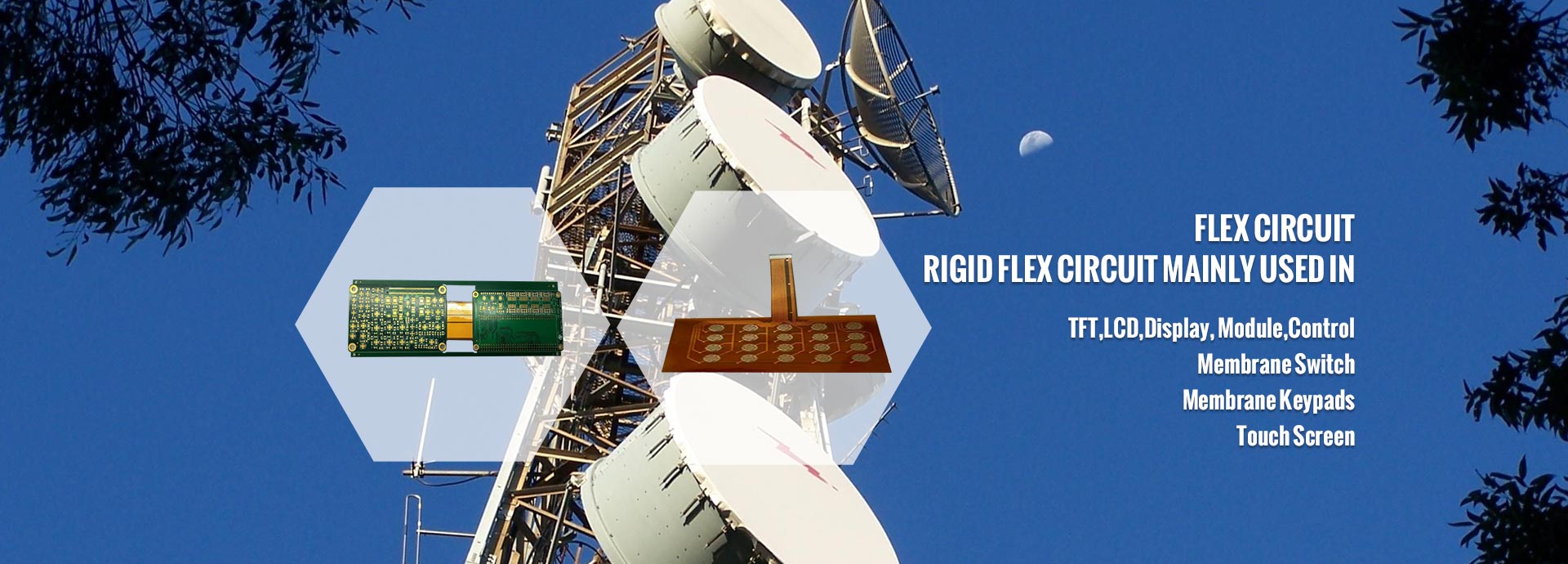
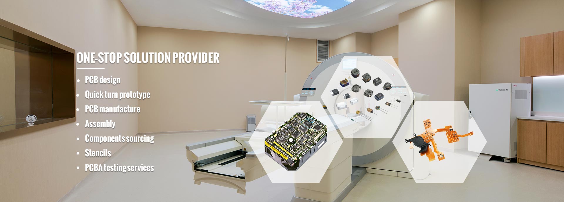
Dear Partners, welcome to MINKINZI – China’s Trusted End-to-End Manufacturing Partner, with 20 years of expertise, we specialize in: Design & Development → PCB Fabrication → PCBA Assembly → Box-Build Assembly. ODM/OEM/Contract Manufacturing tailored to global standards. Support DFM. .

  • OmniAI Modular PCBA Kit

  • OmniAI Modular PCBA Kit

  • OmniAI Modular PCBA Kit

  • OmniAI Modular PCBA Kit

  • OmniAI Modular PCBA Kit

  • OmniAI Modular PCBA Kit

  • OmniAI Modular PCBA Kit

  • OmniAI Modular PCBA Kit

  • OmniAI Modular PCBA Kit

OmniAI Modular PCBA Kit

AI PCBA, smart robotics control board, industrial automation circuit assembly, high-reliability PCB, defect detection technology, IoT hardware solutions, embedded AI systems, custom PCBA manufacturing.

Connectivity: Supports Wi-Fi 6/6E, Bluetooth 5.2, and optional 5G/LTE modules.

Sensors: Compatible with vision, audio, and IoT sensors via standardized I/O ports .

Power: Ultra-low energy consumption (~7.69μJ/inference) for battery-operated devices .


Share

Description :

AI Hardware Core: Critical Roles of FPCs, PCBs, Rigid-Flex PCBs & PCBA in Artificial Intelligence Systems

Discover how advanced printed circuit technologies enable next-generation AI applications across industries. This guide details the specific applications, technical advantages, and stringent requirements for FPCs, Rigid PCBs, Rigid-Flex PCBs, and PCBA in the rapidly expanding AI market.


I. Core Value Proposition for AI Hardware: PCB Technologies Compared

TechnologyKey AI ApplicationsTechnical AdvantagesCutting-Edge AI Example
Flexible PCBs (FPCs)* Foldable AI Device Hinges (Smartphones)
* Wearable Bio-Sensors (ECG Smartwatches)
* Robotic Joint Wiring
Dynamic Reliability: >100,000 bend cycles
3D Space Optimization: Complex routing
Weight Reduction: >30% lighter
Ultra-Thin Micro-FPCs (≤0.1mm) for AR/VR Flexible Displays
Rigid PCBs* AI Server Backplanes (High-Speed Compute)
* Autonomous Driving Controllers
High-Speed: Supports 112Gbps signals (e.g., NVLink)
Low-Loss Materials: Dk≤3.5, Df≤0.002
Robustness: -40°C to 150°C Temp Cycling
18+ Layer Server Boards with Advanced Signal Integrity
Rigid-Flex PCBs* AI Medical Endoscopes
* Drone AI Vision Gimbals
Space & Reliability Solution: 3D packaging + dynamic flex
Vibration Damping
Endoscope Designs: 360° Flex Section + Rigid Imaging Module
PCBA* Miniaturized AI Edge Devices
* High-Power AI Accelerators
Micro-Assembly: 01005 components, 0.3mm pitch BGA
Precision Thermal Mgmt: ±10% tolerance
Signal Integrity: ±5% impedance, <5ps latency
AI Server GPU Accelerator Boards with Advanced Cooling

Growth Insight: The global Rigid-Flex PCB market for AI is projected to reach $2.3 billion by 2025, growing at 12% CAGR.


II. AI Product Scenarios & Critical PCB Requirements

Application AreaAI Product ExampleCritical PCB Technology RequirementKey Driver
Smart HomeAI Learning ThermostatHigh-Temp Metal Core PCB (Teflon Coated)Heat Dissipation in Enclosed Spaces
Smart HealthcarePortable ECG Monitor6-Layer Flexible Sensor Array FPCConformability to Body, Signal Accuracy
Autonomous DrivingLiDAR Perception ModuleVibration-Resistant Rigid-Flex PCBDurability Under Harsh Conditions
Industrial AICollaborative Robot (Cobot)20-Layer High-Tg PCB (Chemical Resistant)Reliability in Demanding Factories

III. Non-Negotiable Factory Requirements for AI PCBs

AI hardware demands exceptional manufacturing quality and capabilities:

  1. Mandatory Certifications:

    • Automotive AI: IATF 16949 Certification

    • Medical AI: ISO 13485 Certification

    • Server Boards: Intel Eagle Stream Certification

  2. Advanced Process Capabilities:

    • AI Server vs. Consumer PCB Requirements:

      ParameterAI Server RequirementConsumer Requirement
      Line Width/Pitch40/40µm (HDI)60/60µm
      Laser Drill Tol.±25µm±50µm
      Impedance Control±5%±10%

(Source: Industry Data Compilation [3][11]22) * Smart Manufacturing: * Real-time MES Monitoring: OEE ≥ 85% * Automatic CTQ Data Collection: 100% * AI-Powered AOI: False Alarm Rate ≤ 0.5%, False Negative Rate ≤ 200ppm


IV. AI OEM Customization Demands for PCB Suppliers

Leading AI developers require factories to deliver beyond basic specs:

  1. Co-Design Expertise:

    • Signal/Power Integrity Simulation Reports (e.g., HFSS Models)

    • Thermal Management Solutions: 3D Simulations + Optimized Material Selection

  2. Supply Chain Resilience:

    • Critical Material Buffer Stock (e.g., ≥30 days for Rogers RO4000)

    • Component Shortage Mitigation (e.g., PCIe4.0 Alternate Compatible Designs)

  3. Agile Execution:

    • Rapid NPI Cycles: ≤15 Days (Design → Prototype)

    • Emergency Order Fulfillment: ≤72 Hour Turnaround

  4. Sustainable Manufacturing:

    • Full RoHS Compliance (Standard 3.0)

    • High-Efficiency Resource Use (e.g., ≥99% Copper Recycling Rate)


Market Outlook & Strategic Recommendations:

  • Explosive Growth: AI Server PCB Market Value Forecast to Exceed $6 Billion by 2025.

  • Technology Shift: Rigid-Flex PCB Adoption in Data Centers Rising to 35% Penetration.

Action Plan for PCB Manufacturers: To capture significant AI market share, prioritize developing these core competencies:

  1. High-Frequency Material Processing: Expertise with low-Dk/Df laminates.

  2. Advanced Micro-Drilling: Consistent ultra-fine via and microvia formation.

  3. Sophisticated System-Level Testing: Ensuring performance under AI workloads.

Invest Now to Power the AI Hardware Revolution!

Blind and Buried Via PCB


Applications :

Blind and Buried Via PCB

PCB & PCBA Solutions for AI Smart Home Devices: A Global Manufacturing Strategy

In the era of Artificial Intelligence of Things (AIoT), printed circuit boards (PCBs) and PCB assemblies (PCBAs) have evolved from passive electronic carriers into intelligent neural backbones that power next-generation smart home ecosystems. As AI-driven devices like voice assistants, robotic vacuums, edge AI cameras, and smart locks become increasingly sophisticated, their performance hinges on advanced PCB/PCBA design, high-precision manufacturing, and resilient global supply chains.

For innovators developing AI-powered smart home products, choosing the right PCB partner isn’t just about cost—it’s about technical alignmenttime-to-market agility, and long-term scalability across global markets.

This comprehensive guide explores:

  1. Key Technical Demands of PCB/PCBA in AI Smart Home Applications

  2. End-to-End Development Process: From Design to Mass Production

  3. Global Manufacturing Landscape: China vs. Southeast Asia vs. Europe & America

  4. How AI Companies Should Choose a PCB Contract Manufacturer – A 3D Decision Model (Time × Cost × Quality)

  5. Why Minkinzi Stands Out: Strategic Advantages of a Truly Integrated Global Manufacturing Network

Let’s dive in.


1. PCB/PCBA in AI Smart Homes: Where Intelligence Meets Hardware

The modern smart home is no longer defined by simple connectivity—it's driven by embedded intelligence. Behind every seamless interaction lies a meticulously engineered PCB platform capable of supporting real-time sensing, machine learning inference, low-power operation, and robust wireless communication.

Smart DeviceCore AI FunctionalityCritical PCB/PCBA Requirements
Smart Speakers
(e.g., Amazon Echo, Xiaomi AI Speaker)
Far-field voice pickup, NLP, cloud integrationMulti-microphone array routing, ultra-low noise power design, EMI shielding, Wi-Fi/BT signal integrity
Smart Door LocksFacial/fingerprint recognition, BLE/Wi-Fi syncHDI (High-Density Interconnect) PCBs, flexible FPCs for sensors/displays, anti-static protection
Home Service Robots
(Robotic vacuum cleaners, companion bots)
SLAM navigation, obstacle avoidance, environmental mappingMultilayer boards with MCU+DSP+NPU architectures, high-speed differential signaling (USB3.0, MIPI), thermal dissipation optimization
Smart Lighting SystemsAdaptive dimming, occupancy detectionMiniaturized SMT processes, constant-current LED drivers, high-temperature-resistant materials (e.g., ceramic substrates)
AI Security CamerasEdge-based human detection, behavior analysisOn-board NPU modules (e.g., Horizon Robotics, Cambricon), PoE power delivery, MIPI CSI-2 interface for image sensors

Deep Insight: With the shift toward edge AI computing, more computational workloads are being processed locally—reducing latency, improving privacy, and minimizing reliance on the cloud. This trend demands PCBAs that support powerful SoCs (e.g., Qualcomm QCS610, Rockchip RK3588) while maintaining long-term stability under thermal stress and electromagnetic interference.

Advanced simulation techniques—including power integrity (PI)signal integrity (SI)impedance control, and stack-up optimization—are now essential for ensuring reliable performance in high-end AI devices.


2. From Concept to Mass Production: The Complete PCBA Solution Lifecycle

Developing an AI smart home product requires more than great software—it needs a seamless hardware development pipeline. For startups and scale-ups without in-house manufacturing capabilities, partnering with a full-service ODM/OEM or EMS provider can dramatically accelerate innovation.

Here’s how a typical AI camera project unfolds within an integrated contract manufacturing ecosystem:

✅ Step-by-Step Development Flow:

  1. Requirements Definition
    Define processing power (TOPS), power budget, size constraints, and target certifications (FCC, CE).

  2. Schematic & Component Selection
    Select AI chipsets (NPU/GPU), memory, image sensors, RF modules—with BOM cost and availability analysis.

  3. PCB Layout & DFM Optimization
    Perform multi-layer stack-up design, impedance matching, and manufacturability checks (Design for Manufacturing / DFT).

  4. Prototype Fabrication & Functional Testing
    Build small batches; assist customers in booting firmware, debugging drivers, and deploying trained AI models.

  5. Supply Chain Integration & Cost Optimization
    Leverage manufacturer’s global procurement network to source alternatives during component shortages.

  6. Automated SMT + DIP Assembly
    Use fully automated lines with SPI, AOI, X-ray inspection for 01005 components, POP stacking, and fine-pitch BGAs.

  7. Reliability Validation
    Conduct temperature cycling (-40°C to +85°C), vibration testing, burn-in aging, and drop tests.

  8. Mass Production & Logistics Management
    Scale up with consistent yield and on-time delivery to regional distribution hubs.

Strategic Value of EMS Partners:
Top-tier contract manufacturers offer "design-in" engineering supportFAI (First Article Inspection) systems, and rapid NPI (New Product Introduction) cycles—effectively acting as an extension of your R&D team. They reduce trial-and-error costs, mitigate risks, and shorten time-to-market by 30–50%.

For AI startups, this partnership model is not optional—it's essential for survival in fast-moving markets.


3. Global PCB Manufacturing Comparison: Choosing the Right Base

With rising geopolitical tensions, trade barriers, and supply chain volatility, leading AI companies are adopting a "China + 1" strategy—diversifying production beyond a single region. Here's a data-driven comparison of key manufacturing regions:

RegionPCB CapabilitySMT LevelCostLead TimeQuality StabilityRisk Profile
Mainland China⭐⭐⭐⭐⭐
World leader in volume & tech maturity (FR-4 to IC substrates)
⭐⭐⭐⭐⭐
Fully automated, supports 01005, POP, μBGA
Medium-Low
Labor/material advantages remain strong
Fast (7-day standard lead)High
Top factories meet IPC Class 3 standards
Medium
Subject to export controls and tariffs
Southeast Asia
(Thailand, Malaysia, Vietnam, Philippines)
⭐⭐⭐☆
Growing mid-tier capacity; limited HDI/advanced tech
⭐⭐⭐☆
Modernizing lines; fewer cutting-edge facilities
Medium
Slightly higher than China; offset by incentives
Medium
Customs/logistics delays possible
Medium
Variability between suppliers
Low-Medium
Primary beneficiary of “China + 1”
Singapore⭐⭐⭐⭐☆
Precision-focused, niche high-reliability boards
⭐⭐⭐⭐☆
Talent-rich, ideal for medical/AI research gear
High
Expensive labor and land
Fast
Efficient customs and operations
Extremely High
Rigorous QC culture
Low
India⭐⭐☆
Underdeveloped infrastructure; inconsistent yields
⭐⭐☆
Skill gap in automation and process control
Medium-Low
Potential future savings
Slow
Infrastructure bottlenecks
Medium
Management systems still maturing
Medium
Frequent policy shifts
North America & Western Europe⭐⭐⭐⭐☆
Specialty focus (military, aerospace, HF boards)
⭐⭐⭐⭐☆
Highly automated but costly
Extremely High
~2–3× Chinese costs
Medium-Slow
Long scheduling lead times
Extremely High
Aerospace-grade compliance common
Low
Dominant for secure/government projects

    Market Trend Outlook:

  • China remains dominant for high-volume, complex PCBA production—especially in the Pearl River Delta and Yangtze River Delta industrial clusters (e.g., Shennan Circuit, USI, Jingwang Electronics).

  • Southeast Asia is rising fast: Thailand (auto-electronics), Malaysia (Intel packaging hub), and Vietnam (TI, Samsung investments) are attracting major PCB players.

  • Singapore excels in high-mix, low-volume premium orders, such as AI medical diagnostics and lab instruments.

  • India shows ambition through its PLI scheme but lacks ecosystem readiness to challenge China at scale.

  • U.S./Europe domestic manufacturing focuses on national security applications—ensuring data sovereignty and supply chain control.


4. How to Choose a PCB Manufacturer? A 3D Decision Framework for AI Innovators

Given this complex landscape, AI companies must adopt a dynamic, lifecycle-aligned sourcing strategy. We recommend the TQC Matrix™—a three-dimensional decision model based on:

  • T: Time-to-Market

  • C: Total Cost of Ownership

  • Q: Quality & Reliability

Recommended Strategy by Product Stage:

Product PhaseRecommended ApproachRationale
Prototype & ValidationPartner with Chinese or Singaporean factoriesRapid turnaround (as fast as 5 days), immediate engineering feedback, access to design-in experts
Pilot Production (NPI)Dual-track: China (primary) + Southeast Asia (backup)Balance speed with risk mitigation; refine processes using mature Chinese ecosystems
Mass Production Ramp-UpImplement "China + Southeast Asia" dual-source modelAvoid U.S. Section 301 tariffs; enhance logistics resilience; diversify geopolitical exposure
Maturity & Global RolloutRegionalize final assembly:
- North America → Mexico/USA
- Europe → Poland/Hungary
- APAC → ASEAN + China
Reduce freight costs, comply with local content rules, pass country-specific certification faster

Additional Evaluation Criteria:

  • Technical Compatibility: Can they handle HDI, any-layer interconnect, embedded passives, or rigid-flex designs?

  • Proven AI Experience: Do they have track records with edge AI platforms (Jetson, Kendryte, Huawei Ascend)?

  • ESG & Regulatory Compliance: RoHS, REACH, carbon footprint reporting required for EU market entry?

  • IP Protection Protocols: NDAs, isolated production lines, encrypted file storage?

Real-World Case Studies:

  • Xiaomi AI Speaker (Global Version): Designed and prototyped in Shenzhen; mass-produced in a Taiwanese-owned SMT facility in Bac Ninh, Vietnam → "Chinese innovation, Southeast Asian execution."

  • Ring Video Doorbell Pro 2: U.S.-led design; SMT assembly in Suzhou, China (Amkor); final assembly in Monterrey, Mexico → Serving North American demand efficiently.

  • Chinese Robotic Vacuum Brand (EU Export): Used Minkinzi’s Malaysian factory for final assembly with China-supplied semi-finished PCBAs → Achieved origin transformation and avoided anti-dumping duties.


5. Why Minkinzi? The Strategic Advantage of a Truly Global Manufacturing Ecosystem

Among the few EMS providers that have successfully built a multi-regional, cross-border manufacturing networkMinkinzi stands out—not just as a factory, but as a strategic enabler for global AI expansion.

   Minkinzi’s Global Footprint:

  • China: Dongguan, Suzhou, Chengdu (Intelligent Manufacturing Hubs)

  • Southeast Asia: Rayong (TH), Penang (MY), Clark (PH), Batam (ID), Ho Chi Minh City (VN)

  • South Asia: Chennai, Pune (IN) (Aligned with "Make in India")

  • Hub Node: Singapore (Regional HQ, R&D Center, High-End Project Command Hub)

Four Key Competitive Advantages:

1. Cross-Regional Production Synergy

All sites operate on a unified ERP/MES system, enabling seamless transfer of process parameters. A reflow profile validated in Dongguan can be replicated exactly in Thailand—ensuring consistency across geographies.

2. Agile Supply Chain Resilience

When Shanghai faced lockdowns in 2022, Minkinzi activated backup lines in Vietnam and Malaysia within 72 hours, preventing customer shipment disruptions—a proven disaster recovery capability.

3. Localized Engineering Support

Each site has dedicated Field Application Engineers (FAEs) and bilingual project managers—enabling real-time troubleshooting, ECN handling, and customer service in native languages.

4. Green Manufacturing Commitment

All facilities are ISO 14001 certified, implementing:

  • Lead-free soldering

  • Wastewater recycling

  • Solar energy adoption Helping clients meet strict ESG goals and qualify for green certifications in Europe and North America.


✅ What This Means for Your Business

Partnering with Minkinzi means gaining more than manufacturing capacity—you gain:

BenefitOutcome
Optimal Cost StructureMatch each market with the most competitive production node
Risk MitigationNever rely on one country again—"don’t put all eggs in one basket"
Fastest Path to MarketParallel prototyping and production across multiple zones
Full Regulatory CoverageOne-stop compliance with FCC, CE, KC, BIS, and other global standards

Final Thoughts: The Future Belongs to Integrated Intelligence & Global Agility

Today’s PCBs and PCBAs are no longer mere circuit boards—they are the nervous systems of artificial intelligence. In a world where software moves at light speed, hardware execution determines who wins.

For Chinese and global AI brands alike, the answer is clear:

❝You don’t need to abandon China—you need to build upon it strategically, then extend globally.❞

A hybrid model of “Chinese foundation + multi-location backup” offers the perfect balance of efficiency, resilience, and scalability.

And when you choose a partner like Minkinzi—with deep roots in China, a growing presence across Southeast and South Asia, and a truly integrated digital backbone—you’re not just outsourcing production.

You’re building a global operation engine.


Conclusion: The Best PCB Factory Isn’t the Cheapest or Fastest…

It’s the one that understands your vision—and walks the entire journey with you.

Whether you're launching your first AI speaker or scaling a fleet of autonomous home robots, your manufacturing partner should be a co-architect of success.

Ready to build smarter, faster, and farther?
Contact Minkinzi today to unlock a new era of intelligent hardware innovation—powered by precision PCB/PCBA solutions and a borderless manufacturing future.

Flow Chart :


Blind and Buried Via PCB

Blind and Buried Via PCB

Blind and Buried Via PCB

Blind and Buried Via PCB

Blind and Buried Via PCB

Blind and Buried Via PCB

Blind and Buried Via PCB

Blind and Buried Via PCB

Blind and Buried Via PCB

Blind and Buried Via PCB

Blind and Buried Via PCB

Blind and Buried Via PCB

Blind and Buried Via PCB

Blind and Buried Via PCB

Blind and Buried Via PCB

Comprehensive Guide to AI Product Development: From Design to Mass Production (2025)

The journey from concept to mass production of intelligent AI-powered hardware products involves a multi-disciplinary approach spanning system architecture, embedded engineering, algorithm optimization, supply chain strategy, and scalable manufacturing. This definitive guide outlines the end-to-end process of AI product development, highlights real-world applications across industries, and provides actionable insights into material selection, compliance, and cost-efficient scaling—ideal for innovators building next-generation edge AI devices.


I. The 5-Stage AI Product Development Lifecycle

1. Solution Architecture & Requirements Engineering

Before writing a single line of code or placing a component on a PCB, successful AI products begin with clear functional goals and performance KPIs:

  • Functional Scope: Define use cases (e.g., real-time object detection, voice-controlled automation).

  • Performance Targets: Specify inference latency (<100ms), power budget (<5W), thermal envelope, and environmental durability.

  • Chipset Selection Strategy:

  • Edge Devices: NVIDIA Jetson Orin Nano / Google Coral TPU — ideal for prototyping.

  • High-Performance Systems: Custom ASICs (like Tesla’s FSD chip) for optimized autonomy workloads.

  • Framework Alignment: Choose between TensorFlow, PyTorch, or ONNX based on model portability and deployment ecosystem.

✅ Pro Tip: Use modular architecture early—decouple sensor input, compute engine, and output control to accelerate iteration.


2. Hardware Development: Advanced PCB Design & Material Selection

Robust hardware forms the backbone of any reliable AI device. Key focus areas include signal integrity, thermal management, and long-term reliability.

High-Speed PCB Design Best Practices

FeatureSpecification
Layer Count8–12 layers for high-density routing
Impedance Control±10% tolerance for MIPI, PCIe, DDR interfaces
Thermal ManagementEmbedded copper vias, thermal pads under BGA chips
EMI ShieldingGround planes, Faraday cage design for RF-sensitive modules

Core Component Selection Guide (With Real-World Applications)

ComponentRecommended Brands/ModelsApplication Examples
AI Accelerator ChipsNVIDIA Jetson AGX Orin, Google Edge TPU, Hailo-8Smart cameras, mobile robots
Wireless SensorsBroadcom BCM43xx Wi-Fi/BT, Infineon radar sensorsSmart homes, presence detection
Memory & StorageSamsung LPDDR5, Kioxia eMMC/UFSAI voice assistants, dashcams
Power Management ICsTexas Instruments TPS series, Analog Devices LTCIndustrial AI gateways, drones
Camera ModulesSony IMX series (IMX586, IMX708)Facial recognition, AR/VR systems

Critical Note: Always validate component availability over a 3–5 year horizon. Single-source parts can cripple scalability.


3. Software & AI Algorithm Development

While hardware enables performance, software defines intelligence. A holistic development pipeline includes:

Model Training & Optimization

  • Use domain-specific datasets (e.g., retail foot traffic, medical imaging).

  • Apply data augmentation and active learning to reduce labeling costs.

  • Optimize for sparsity, quantization (INT8), and pruning to enable edge deployment.

Embedded Deployment Stack

ToolPurpose
TensorFlow Lite / PyTorch MobileOn-device inference
TensorRT / OpenVINOHardware-accelerated execution
ROS 2 (for robotics)Sensor fusion and navigation stack

Fact: Poor data quality accounts for up to 70% of AI model failures in production (McKinsey, 2024). Invest in clean, diverse, and ethically sourced training data.


4. Manufacturing: SMT Assembly & System Integration

Transitioning from prototype to volume production requires precision and process control.

Surface Mount Technology (SMT) Process Highlights

  • Placement Accuracy: ±0.01mm for 0201 passives and fine-pitch BGAs.

  • Void Rate Control: ≤0.5% in BGA solder joints via nitrogen reflow.

  • Quality Assurance Tools:

    3D SPI (Solder Paste Inspection)

  • AOI (Automated Optical Inspection)

  • X-ray CT scanning for hidden joint analysis

Enclosure & Mechanical Design

RequirementSolution
Heat DissipationDie-cast aluminum chassis, heat pipes
Lightweight DesignReinforced polycarbonate or PBT+GF30 plastic
Environmental ProtectionIP54/IP67 sealing for dust/water resistance
EMI ComplianceConductive gaskets, shielded connectors

Case Insight: Industrial AI inspection robots often combine magnesium alloy frames with conformal coating to survive harsh factory environments.


5. Testing, Validation & Mass Production Ramp-Up

Final validation ensures field reliability and customer satisfaction.

Functional & Stress Testing Matrix

Test TypeParameters
Environmental-40°C to +85°C operating range, 95% RH humidity
Vibration/ShockMIL-STD-810G compliant (drones, automotive)
Longevity Burn-in72–168 hours at full load
AI Performance BenchmarkInference speed, accuracy (F1 ≥ 95%), false positive rate

Scaling to Mass Production

  • First-Pass Yield Goal: >99% through statistical process control (SPC).

  • Pilot Run → Full Volume: Lock down firmware, test jigs, calibration procedures.

  • Supply Chain Buffering: Stockpile critical ICs (GPUs, PMICs) for 6 months to mitigate global shortages.

Conversion Boost: Include traceability (UUID per unit), OTA update capability, and remote diagnostics—features that increase perceived value and reduce after-sales cost.


II. Top 10 High-Impact AI Product Applications (Ranked by Market Adoption & ROI)

These are the most commercially successful AI-powered solutions driving innovation across sectors in 2025:

RankAI Product CategoryCore TechLeading Use CasesAnnual Growth
1Autonomous Driving Domain ControllerNVIDIA DRIVE Orin + LiDAR/Stereo FusionTesla, XPeng, NIO28% CAGR
2AI Vision Security CameraHiSilicon Hi3519 + YOLOv8Smart cities, retail analytics24%
3Medical Imaging DiagnosticsIBM Watson AI + RadiomicsCancer screening (↑30% detection)31%
4Industrial Quality Inspection RobotDeep Learning + Line Scan CamerasPCB defect detection (99.35% accuracy)26%
5Smart Home HubXiaomi Xiaoai / Amazon Alexa + NLPVoice-controlled IoT ecosystems19%
6AI Education Companion RobotiFlytek Emotional AI + Adaptive LearningPersonalized tutoring, language practice22%
7Agricultural DronesIntelinAir AI + Multispectral ImagingCrop health, soil fertility mapping35%
8Financial Risk Control SystemXTransfer Large Model + Anomaly DetectionCross-border fraud prevention40%
9Virtual Digital HumanLemon Slice One-Shot GenAICustomer service avatars, metaverse$10.5M funding raised
10AI Wearables (Health Monitoring)Apple Watch ECG + ML anomaly predictionEarly warning for atrial fibrillation27%

 "AI security camera," "industrial AI robot," "edge AI device," "AI wearables 2025"


III. Critical Success Factors in AI Product Commercialization

Beyond technical excellence, strategic decisions determine whether an AI product scales profitably.

1. Regulatory Compliance & Global Certification

Ensure adherence to regional standards early:

  • CE/FCC/IC: Mandatory for wireless consumer electronics (EU/US/Canada).

  • FDA 510(k): Required for AI diagnostic tools in healthcare.

  • UN R155/R156: Cybersecurity & software updates for automotive AI.

Non-compliance risks market entry delays and legal liability.

2. Supply Chain Resilience Strategies

  • Adopt dual-sourcing for GPUs, MCUs, and memory chips.

  • Qualify alternative suppliers in ASEAN or Eastern Europe.

  • Leverage consignment inventory models with contract manufacturers.

3. Cost Optimization by Volume

Production StageCost Strategy
Prototyping (<1K units)Use FPGA or off-the-shelf SoMs (e.g., Toradex)
Mid-volume (1K–50K)Optimize layout; negotiate JDM partnerships
Mass Production (>50K)Migrate to custom ASIC or ASSP to cut BOM by 30–50%

Example: Tesla saved ~$200/unit by transitioning from GPU-based prototypes to custom Dojo-trained FSD chips.

4. Fast Iteration via Modular Design

Break systems into interchangeable modules:

  • Compute module (removable SoM)

  • Sensor pod (plug-and-play interface)

  • Power bank (hot-swappable)

Enables hardware iterations in under 3 days, crucial for agile startups competing with big tech.


Final Thoughts: Building Scalable, Future-Proof AI Products

Developing a successful AI product isn't just about deploying deep learning—it's about integrating intelligent designrobust engineering, and strategic operations into every phase. Whether you're launching an AI camera, autonomous robot, or wearable health monitor, this framework ensures:

✅ Faster time-to-market
✅ Higher yield and reliability
✅ Stronger investor and customer confidence

By aligning technical decisions with business goals, leveraging proven components, and anticipating regulatory and supply risks, you position your AI innovation not only to rank highly on Google but also to dominate its market segment.


Want More? Download Our Free Checklist:
"10 Must-Have Features in Every AI Hardware Product"

Capability :

Blind and Buried Via PCB

Minkinzi: Premier AI Hardware Manufacturing Partner for End-to-End PCBA & System Integration

Accelerating AI Innovation with 99.9% Yield Rate & Million-Scale Monthly Capacity


I. Cutting-Edge Manufacturing Capabilities

1. High-Complexity PCB/PCBA Solutions

  • Advanced Process Tech:

  • 10-40 layer HDI PCBs • Substrate-like PCBs (SLP) • Flex/Rigid-Flex Boards

  • Precision: ≤3.5mil line width • 0.2mm±0.05mm thickness tolerance

  • AI-Driven QA: 100% automated component inspection (e.g., Xiaomi Wuhan Smart Factory)

  • Scalable Capacity:

  • Prototyping: 24-hour expedited / 72-hour standard delivery

  • Mass Production: 99.9% smart factory yield • 1M+ units/month (e.g., Xiaomi AC line: 6.5s/unit)

2. High-Precision SMT & Assembly

  • Micro-Component Handling: 01005 chips • 0.3mm-pitch BGAs

  • Cobot-Driven Lines: Zero-defect embodied intelligence assembly (Intel × Fulin model: 800 cases/3hr)

  • Mixed-Product Flexibility: 6 parallel product lines (Changhong-certified)


II. Proven AI Hardware Success Cases

✅ AI Computing Systems

  • GPU accelerator PCBA for NVIDIA • Server PCBA for Alibaba/Tencent (Zhuhai Xingsen Tech)

✅ Embodied Intelligence

  • Humanoid Robot Joints: Full PCBA for UBTECH & Unitree

  • Industrial Cobots: Intel × Anlu control boards

✅ Smart Wearables

  • TWS/AR Glasses: Goertek/ByteDance eyewear assembly (Luxshare Precision)

  • Biocompatible Health Tech: Huami bracelets with medical-grade substrates


III. Supply Chain Advantages for AI Devices

MaterialImported BrandDomestic AlternativeCost/Delivery Edge
High-Frequency PCBRogers RO4000 (US)Shengyi SY Series (CN)20% cost ↓ • 8-week delivery ↓
Flexible CircuitsNippon Mektron (JP)China FPC Solutions8090/(vs.120)
Bio-SensorsDuPont Pyralux (US)CLCP Series (CN)Stock availability
Micro-BatteriesTDK (JP)EVE Energy (CN)15% cost ↓ • 2-week faster

Key Competitive Edges:
Global Sourcing Network: 800+ suppliers (TI/Murata OEM partnerships) • 100K+ SKUs in stock
Cost Control: 30% BOM reduction via centralized procurement + domestic substitution (AiPCBA model)
Tariff Mitigation: SE Asia/Mexico hubs for duty-free NA/EU exports (e.g., Minkinzi Vietnam)


IV. Intelligent Production & Delivery Assurance

AI-Optimized Manufacturing

  • Digital Twin QA: Defect rate ↓30-50% (Changhong Energy battery line)

  • Dynamic Scheduling: 11-day cycle optimization (Changhong model)

Global Delivery Network

  • China: Yangtze/Pearl River Delta clusters (24hr logistics radius)

  • Worldwide: Vietnam/Hungary factories (0-tariff to EU/US)

Certifications:
ISO13485 (Medical) • IATF16949 (Automotive) • AEC-Q200


V. Strategic Cooperation Paths

  1. Complex AI Hardware → Opt for substrate+HDI experts (Minkinzi’s 40-layer PCB capability)

  2. R&D Prototyping → Leverage 24hr-quote services (AiPCBA platform)

  3. Cost-Sensitive Wearables → Adopt domestic material chains (e.g., Lens Tech/Lingyi solutions)


Why 200+ AI Clients Choose Minkinzi:

"From NVIDIA GPUs to ByteDance AR glasses – we deliver faster time-to-market through integrated design-for-manufacturing (DFM), risk-proofed supply chains, and smart factory scalability."

[Request Customized Quotation] | [Schedule Virtual Factory Tour]

Advantages :

Minkinzi: Your End-to-End AI Hardware Manufacturing Partner

From Concept to Certified Deployment – Precision Engineered for AI Innovation

I. Core Capabilities That Accelerate AI Deployment
Full-Stack Technology Integration

  • AI-Optimized Design: Chipset support (NVIDIA Jetson/Qualcomm RB5), sensor fusion architecture & edge computing solutions

  • Agile Manufacturing: AI-powered low-code platforms (e.g., Foxconn Fii) enable minute-scale line changeovers for high-mix, low-volume batches

Deep Supply Chain Control

  • 100,000+ pre-certified components including NVIDIA H100/A100 GPUs, Cambricon MLUs

  • Co-development partnerships with chip innovators (e.g., MaPU architecture with Silang Tech)

Intelligent Production Systems

  • MES-tracked precision: ±25μm placement accuracy with >90% OEE equipment efficiency

  • Closed-loop quality control from SMT to final test

II. Military-Grade Validation Infrastructure

Test PhaseCutting-Edge EquipmentCritical SpecificationsProven Applications
SMT Production3D SPI Solder Paste Inspectors≤10μm resolution, ≥20cm²/s speedHydrogen fuel cell MEA inspection (MIRVY)
Solder IntegrityMicrofocus X-Ray Systems≤1μm resolution, <15% BGA void rateAI server PCB validation (JL Technology)
Functional ReliabilityGHz-Speed Flying Probe + ICT Testers>1GHz frequency, 1024+ channelsFull motherboard testing (Foxconn FII)
Environmental RobustnessThermal Cycle Chambers-40℃~150℃, 10-98% RHAutomotive AI controllers (AEC-Q100 certified)
Vision AI QADeep Learning AOI Systems>99.5% defect detectivity, <0.1% false callsIndustrial camera modules (Advantech)

III. Globally Recognized Compliance

  • Quality Systems: ISO 9001 + IATF 16949 (Auto) + ISO 13485 (Medical) + IPC-A-610H Class 3 (Military Electronics)

  • Product Safety: UL 62368-1, EN 55032 (EMC), IEC 62133 (Battery Safety)

  • Ethical AI Governance: GDPR + ISO 27001 + China’s Generative AI Security Requirements

IV. Industry-Proven AI Solutions
Hyperscale AI Servers

  • Liquid-cooled GPU racks for cloud providers (48hr/85℃ full-load validated with Foxconn FII)

  • Autonomous Driving Controllers

  • ASIL-D compliant L4 domain controllers (MTBF >100k hrs, AEC-Q100 certified)
    Medical AI Diagnostics

  • FDA 21 CFR Part 820-compliant PCBs for CT/X-ray systems (MILFIT case)
    Secure Edge AI Devices

  • ARM TrustZone embedded systems with SESIP L3 security certification

V. Future-Ready Manufacturing
Sustainable Tech: RoHS 3.0 & REACH SVHC compliance (lead-free processes)
AI-Driven Efficiency: NVIDIA Modulus-powered simulations (700,000x faster R&D iteration)

Materials :

Minkinzi: Your End-to-End AI Hardware Manufacturing Partner - From Advanced PCB Design to Scalable Production

Optimized for Performance, Precision & AI Innovation

Minkinzi empowers AI innovators with comprehensive hardware solutions, seamlessly integrating cutting-edge PCB design, advanced PCBA manufacturing, and robust module development. Leveraging deep expertise and state-of-the-art facilities, we accelerate your AI solutions from concept to high-volume production.

I. Advanced PCB Design & Fabrication Expertise:

  • High-Speed, High-Layer-Count PCBs: Expertise in ≥20-layer boards (up to 40+ layers), featuring ultra-fite 3mil trace/spacing (0.076mm), tight ±5% impedance control, and low-loss materials (e.g., Panasonic M6G/M7N1).
    Proven In: AI Server Motherboards (e.g., Huadian Tech: 800G optical module support), GPU Accelerator Cards (e.g., Leading AI Co. designs), Data Centers, HPC, Optical Modules.

  • High-Frequency/RF PCBs: Superior signal integrity with Dk stability ±0.05 (PTFE substrates), ultra-low loss ≤0.8dB/cm@10GHz.
    Proven In: Satellite Comms (AI-optimized routing achieving -45dB crosstalk).

  • HDI & Flexible PCBs: 1st-3rd order microvias (≤0.1mm diameter), >100k bend cycles for dynamic applications.
    Proven In: Smart Wearables (e.g., Hausen Intelligent Robot Control Board).

II. Precision PCBA Manufacturing & Processes:

  • High-Density SMT Assembly: 01005 component placement (±25μm)100% 3D SPI coverage0.3mm BGA capability.
    Proven In: AI Edge Computing Modules (e.g., OEM for Panasonic Electromechanical AI servers).

  • Advanced Thermal Management: Engineered solutions with ≥5W/mK thermal conductivity (metal core), <0.5°C/W thermal resistance (vapor chambers).
    Proven In: High-Reliability GPU Cooling PCBA Mass Production (Minkinzi Electronics).

III. Core AI Hardware Module Development:

  • AI Acceleration Modules: PCIe 5.0 support300W~700W TDPHBM2e integration.
    Proven In: Inspur AI Factory (Scaled production of 1000+ annual models).

  • Edge Computing Devices: ≥10 TOPS NPUROS compatibility±5cm SLAM accuracy.
    Proven In: Autonomous Driving Platforms (e.g., Anhui Mech. & Elec. Eng. College).

  • Sensor Fusion Modules: Multi-modal integration (IMU+LiDAR+Vision)<10ms ultra-low latency.

IV. State-of-the-Art Manufacturing & Quality:

  • Intelligent Factory: SMT CPK ≥1.67AOI false alarm rate <1%Digital Twin simulation.
    Proven In: Minkinzi Humanoid Robot Line (Walker S2 iteration in 9 months).

  • Rigorous Testing & Certification: Signal Integrity @56Gbps, Full EMC/Safety Compliance (CE/FCC/UL).

V. Specialized Materials & Enclosures:

  • Premium PCB Materials: High-Frequency Laminates (Rogers RO4000), Ceramic Substrates (AlN).

  • Robust Industrial Enclosures: IP67 protection≥60dB EMI shieldingLiquid cooling integration.
    Proven In: Booster AI Voice Mouse (Ergonomic + Multi-Device Compatible).

VI. Demonstrated Success Across AI Sectors:

SectorProject ExampleKey Technical Achievement
AI ServersShennan Circuits 800G Optical Module112Gbps channelsLoss <0.3dB/inch
Industrial RobotsHausen Tightening/Welding RobotsSupports 40+ structured tasks
Smart TerminalsYunjue VITA AI Glasses 3Zero-code trainingAIGC large model deploy
Autonomous DrivingL4 Edge Computing TerminalMulti-sensor fusion<50ms obstacle response

Certified Quality & Compliance: ISO 9001IATF 16949 (Automotive)RoHSREACH.

Why Partner with Minkinzi for AI Hardware?

  • Full Supply Chain Integration: Seamless journey from design simulation to mass production.

  • AI Factory Agility: Proven high-mix, high-volume capability (1000s of orders/year).

  • Closed-Loop R&D to Production: Accelerate your time-to-market with our integrated expertise.

  • Performance-Driven Solutions: Hardware engineered for the extreme demands of AI compute, edge, and sensing.

Ready to Build the Future of AI Hardware?

Contact Minkinzi today for a consultation on your next-generation AI project!

Materials :

OmniAI Modular PCBA Kit

Minkinzi Factory: Your Premier AI Hardware Manufacturing Partner for High-Speed PCB & PCBA Solutions

Specializing in AI Computing Modules, Edge Devices & Sensing Systems

Core Capabilities at a Glance

✓ High-Frequency/High-Speed PCBs
✓ Rigid-Flex & Multilayer Boards (2-36L)
✓ End-to-End PCBA & Box Build
✓ Agile NPI Prototyping to Mass Production
✓ AI-Optimized Manufacturing (SMT, Selective Soldering, Advanced DFM)


Why Global AI Innovators Choose Minkinzi

Elite Material Selection & Guaranteed Inventory

High-frequency boards stocked for 7-day delivery:

  • Panasonic R-5785/R-5670 (Dk 3.48, Df 0.0027)

  • Rogers RO4350B (Industry benchmark for RF)

  • Domestic Alternatives: Tayohu TH-55P (Dk 3.52, Df 0.0032)
    ✅ 500+㎡ monthly stock | ✅ 18"x24" panels | ✅ Cost-performance optimization

Dual-Source Component Ecosystem

Mitigate supply chain risks with international/domestic partners:

CategoryGlobal BrandsDomestic Alternatives
Solder PasteIndium 8.9HF (<3% voids)Yichengda ECTC-880LF
RCL ComponentsMurata AEC-Q200Fenghua/Yuyang Auto-grade
ICsTI, InfineonSGMICRO/Southchip
ConnectorsMolex/TE ConnectivityAVIC/Tyco Custom molds
✅ Anti-collapse pastes ✅ -40℃~125℃ operation ✅ EMI/IP54 enclosures

Precision Soldering Technologies

Boost yield with industry-leading processes:

  • Nitrogen Wave Soldering: <50ppm O₂ → 98.6% hole fill rate

  • Selective Soldering: AOI-guided robots → <80 PPM defects

  • Reflow Control: KIC-verified profiles for BGA/QFN

Rigid-Flex PCB Mastery

For wearables, AR/VR & foldable AI:

  • Materials: DuPont Pyralux coverlays + Kaneka PI substrates

  • RA Copper Foils: 12-18μm for 200k+ bend cycles

  • Laser Microvias: R=1.5mm min. bend radius
    ✅ ENEPIG/ENIG finishes ✅ Mass-proven in smart glasses/bracelets

Quality & Speed DNA

  • Traceability: MES-tracked per-board ID + component-level scanning

  • DFM Collaboration: Free PI/thermal simulations & stackup reviews

  • Agile Delivery: 7-day turnaround for ≤500pcs | MOQ=1


Partner Benefits for AI Hardware Teams

"We accelerate reliable hardware deployment for algorithm-driven markets where milliseconds matter – from autonomous perception systems to edge inference engines."

Competitive EdgeYour ROI
✦ 3-month material buffers→ Zero supply-chain downtime
✦ Domestic alternatives→ 18-35% BOM cost reduction
✦ Closed-loop process control→ 40% lower field failures
✦ NPI-phase daily updates→ 50% faster market entry

Unlock Your AI Hardware Advantage

Free Resources for OEM/ODM Teams:
① [Download] High-Frequency Material Dk/Df Comparison Kit
② [Get] SMT Stencil Design Specs V2.3
③ [Request] Rigid-Flex Stackup Design Handbook
④ [View Case Studies] AI Voice Boxes • Drone Controllers • Edge Servers

Next Step: Contact our AI Solutions Manager for:
24-hr DFM Feedback ✦ Live Factory Tour ✦ Prototyping Coupon


Stay Ahead in AI Hardware:
#PCBAManufacturing #HighSpeedDesign #EdgeComputing #AIIoT #RigidFlexPCB

Knowledge

Contact Us

Telephone: +86 0769 3320 0710

Cel/What's app: +86 134 6956 5519

sales@minkinzi.com

www.minkinzi.com

Address 1:Songshan Lake International Creativity Design Industry Park,No. 10, West Industrial Road,Songshan Lake High-Tech Dist.,Dongguan,China.523808. Address 2:No. 18, Zhenyuan East Road, Chang 'an Town, Dongguan City, Guangdong Province.523000.

Copyright ©Minkinzi Circuit Technology Co., ltd. ZhiYi Electronic All Rights Reserved | Sitemap