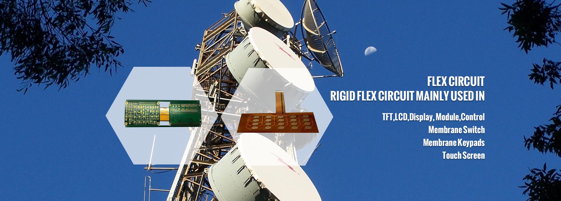
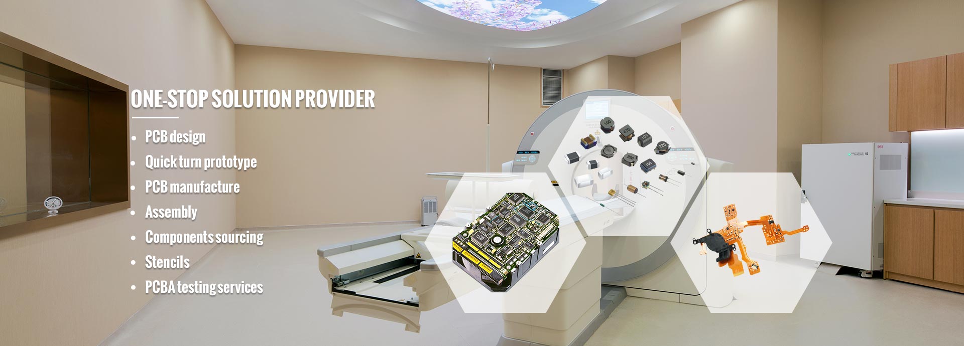
Dear Partners, welcome to MINKINZI – China’s Trusted End-to-End Manufacturing Partner, with 20 years of expertise, we specialize in: Design & Development → PCB Fabrication → PCBA Assembly → Box-Build Assembly. ODM/OEM/Contract Manufacturing tailored to global standards. Support DFM. .

  • High-Performance 5G 6G PCB Assembly | Scalable Telecom Solutions

  • High-Performance 5G 6G PCB Assembly | Scalable Telecom Solutions

  • High-Performance 5G 6G PCB Assembly | Scalable Telecom Solutions

  • High-Performance 5G 6G PCB Assembly | Scalable Telecom Solutions

  • High-Performance 5G 6G PCB Assembly | Scalable Telecom Solutions

High-Performance 5G 6G PCB Assembly | Scalable Telecom Solutions

5G/6G PCBA - Next-Gen Connectivity Solutions

Accelerate Innovation with Cutting-Edge Circuitry


⚡ Ultra-High-Speed Performance

Engineered for 5G (100Mbps–1Gbps) and future 6G networks, our PCBAs deliver 10x faster data transmission vs. legacy systems. Supports real-time IoT, autonomous vehicles, and industrial automation with near-zero latency.


Share

Description :

High-Performance 5G 6G PCB Assembly | Scalable Telecom Solutions

Unlocking 5G/6G Success: Advanced PCB/PCBA Solutions for Next-Gen Communication Demands

The relentless evolution towards 5G deployment and 6G research places unprecedented demands on the foundational technologies enabling high-speed, low-latency, and ubiquitous connectivity. Manufacturers of Flexible Printed Circuit Boards (FPCs), Rigid Printed Circuit Boards (PCBs), Rigid-Flex PCBs, and PCB Assemblies (PCBAs) are pivotal to this transformation. This analysis systematically details their critical roles, real-world applications, and the stringent requirements communication customers impose.

I. Mission-Critical Roles in 5G/6G Infrastructure

  1. Rigid-Flex PCBs: Miniaturization & Dynamic Reliability

    • Core Value: Enables compact device design and robust performance under stress. Rigid sections house components while flexible segments allow dynamic bending, solving complex spatial constraints inherent in advanced communication devices.

    • Key Applications: 5G smartphone antenna modules (e.g., mmWave), dense signal routing in Base Station RRUs, vibration-resistant satellite communication hardware.

    • Precision Specs: Interlayer alignment ≤50μm, blind via diameter ≥0.1mm, bend radius ≥3x board thickness.

  2. High-Frequency Rigid PCBs: Powering Bandwidth & Speed

    • Core Value: Supports high-power, ultra-high-bandwidth signal transmission with minimal loss and efficient thermal management.

    • Material Science: Base Stations: PTFE/ceramic-filled substrates (Dk≤3.5, Df≤0.003). Servers: 20+ layer boards with embedded capacitors (reducing signal loss by 40%).

    • Critical Use Cases: AI server GPU substrates, high-speed optical module backplanes.

  3. Flexible PCBs (FPC): Enabling Mobility & Innovation

    • Core Value: Provides essential flexibility and lightweight connectivity for next-generation portable and wearable communication devices.

    • Advanced Materials: LCP (Liquid Crystal Polymer) replacing PI (Df≤0.002 @ mmWave), enabling superior high-frequency performance.

    • Application Spotlight: Interconnects in AR/VR headsets, sensor networks in smart wearables.

II. Real-World 5G/6G Applications Powered by PCBs

Application DomainKey PCB Technology EnablersUser-Centric Scenarios
Smart Home/IoTUltra-Low Latency PCBA (≤1ms) + Edge ComputeSeamless thermostat control, security alerts
Vehicle-to-Everything (C-V2X)Automotive-Grade Reliability (Failure Rate ≤10⁻⁹/hr)Real-time traffic data, autonomous driving
Industrial IoTExtreme Temp PCBs (Tg≥200℃) + 5G Private NetsRemote equipment diagnostics, predictive maintenance
Smart HealthcareLow-Radiation FPC + Secure 5G TransmissionWearable health monitors, remote surgery aid

III. Top 7 Requirements from Communication Customers

Communication OEMs demand PCB/PCBA partners meet these critical benchmarks:

  1. Material & Process Excellence: Certified high-frequency laminates (e.g., Rogers RO4350B), ultra-tight tolerances (mmWave linewidth ≤±1μm, impedance ±5%), military-grade rigid-flex lamination (offset ≤25μm).

  2. Advanced Thermal & Signal Management: Embedded copper heatsinks (reducing junction temps by 25°C in 5G RRUs), R&D focus on ultra-low loss substrates for 6G (Df≤0.001@1THz).

  3. Smart Manufacturing Prowess: Integrated MES for traceability (yield ≥98.7%), AI-optimized processes (e.g., LDI imaging boosting line qualification to 99.5%).

  4. Uncompromising Reliability: Rigorous testing protocols (Automotive: -40°C~125°C thermal cycling x3000 + 500hr salt spray; Industrial: vibration resistance ≥100g).

  5. Sustainability & Compliance: Strict adherence to RoHS 3.0 lead-free standards, high-efficiency waste recovery (Cu²⁺ ≥99%).

  6. Supply Chain Agility: JIT delivery capabilities (72hr rapid-turn), comprehensive design-to-test solutions (e.g., SiP integration).

  7. Certified Quality Systems: IATF 16949 (Automotive), AS9100D (Aero), backed by accredited lab failure analysis (e.g., Minkinzi Circuits).

IV. Meeting the 6G Horizon: Future-Proofing Manufacturing

Staying ahead requires tackling emerging challenges:

  • Material Innovation: Nano-cenhanced PTFE (Dk≤1.8, temp resistance 300°C+).

  • Radical Integration: Terahertz band PCB-chip embedding (80% signal path reduction).

  • Digital Transformation: Virtual factory twins optimizing cycles (15% cost reduction, 30% fewer defects).

Industry Leadership Examples:

  • Anjielimei Vivi: Smart factory mastering packaging substrates & premium HDI.

  • Minkinzi Circuits: Aviation-grade hybrid boards (C919 avionics) using loss-reducing buried capacitors (-40% loss).

Conclusion: The Path Forward for PCB Manufacturers The communication sector's relentless drive demands a triad of excellence from PCB/PCBA suppliers: mastery of high-frequency materials science, precision at the nanoscale process level, and adoption of digital twin manufacturing. To capture market share in the 5G/6G era, factories must simultaneously build deep technical expertise, invest in advanced capabilities, and demonstrate proven results like the benchmark cases above. Partner with manufacturers equipped for the future of connectivity.

Applications :

High-Performance 5G 6G PCB Assembly | Scalable Telecom Solutions

The Strategic Role of PCBs & PCBAs in 5G, 6G, and Next-Generation Telecommunications: A Global Outlook on Technology, Manufacturing, and Supply Chain Innovation

As the world accelerates into the era of ultra-high-speed wireless communication, Printed Circuit Boards (PCBs) and Printed Circuit Board Assemblies (PCBAs) have evolved from passive interconnect components into mission-critical enablers of modern telecom infrastructure. In both 5G deployment and emerging 6G research, PCB/PCBA performance directly influences signal integrity, thermal efficiency, power delivery, electromagnetic compatibility (EMC), and system-level reliability across base stations, edge computing nodes, satellite terminals, and intelligent devices.

This comprehensive guide explores five pivotal dimensions shaping the future of telecom-grade PCB solutions:

  1. 20+ Real-World Application Scenarios of PCBs/PCBAs in 5G/6G Networks

  2. Advanced Design & Development Requirements for High-Frequency, High-Speed Systems

  3. Global OEM/ODM Manufacturing Landscape: Competitive Analysis Across China, Southeast Asia, and North America/Europe

  4. How to Choose the Right PCB & SMT Partner: A Data-Driven “Time-Cost-Quality” Decision Framework

  5. Case Study: Minkinzi’s Global Manufacturing Strategy – Bridging Innovation with Scalability

Let’s dive deep into each domain — combining engineering precision with strategic insight.


I. 20+ Critical Applications of PCBs & PCBAs in 5G, 6G, and Modern Telecom Infrastructure

With data rates exceeding 800 Gbps in optical modules and frequencies pushing into the terahertz (THz) range for 6G R&D, traditional PCB materials like standard FR-4 are obsolete. Instead, next-generation communication systems demand ultra-low-loss laminateshigh-density interconnects (HDI)impedance-controlled routing, and advanced thermal designs.

Below are 20+ key application areas, categorized by technology segment and product type, where PCB/PCBA innovation drives real-world performance:

No.Technology DomainProduct TypeKey PCB/PCBA Characteristics
15G Macro Base StationActive Antenna Unit (AAU)12–20 layer high-frequency board; Rogers/Isola materials; millimeter-wave support; HDI design
2Small Cell NetworksMicro/Pico/Femto CellsMiniaturized RF-digital hybrid PCBs; low-power optimization; embedded filtering
36G Research PlatformsTerahertz (THz) Transceiver Module>100 GHz operation; LTCC or flexible substrates; phase-stable signal paths
4V2X ConnectivityAutomotive Millimeter-Wave RadarDifferential pair routing at ±5% impedance tolerance; EMI shielding; ruggedized layout
5Optical Networking400G/800G QSFP-DD DR4 ModulesMegtron7-based PCBs; controlled dielectric thickness; co-packaged optics readiness
6Core Network5G UPF Server20–32 layer backplanes; PCIe Gen5; high-speed SerDes channels
7Edge ComputingMulti-access Edge Compute (MEC) GatewaysMixed-signal integration (RF + Digital + Power); active cooling design
8Satellite CommunicationsPhased Array Antenna Terminals (e.g., Starlink)Microwave-frequency boards; beamforming IC substrates; lightweight structural PCB
9Intelligent TransportC-V2X Onboard UnitsAEC-Q200 qualified assembly; wide temp (-40°C to +85°C); vibration resistance
10IoT EcosystemNB-IoT/LTE-M Sensor GatewaysUltra-compact SMT design; minimal power consumption; chip-scale packaging
11Data CentersToR/Spine Switch Motherboards≥56 Gbps PAM4 signaling; PI/SI co-simulation; blind/buried vias
12Baseband ProcessingBBU with CU/DU Split ArchitectureFPGA + ASIC co-layout; high I/O BGA escape; thermal pad integration
13RF Front-EndPower Amplifier & Filter ModulesMicrostrip/stripline topologies; ground plane continuity; RF isolation
14Frequency ControlSAW/BAW FiltersCeramic/glass substrate packaging; nanoscale etching accuracy
15Advanced PackagingBeamforming IC Substrates (SiP)Embedded passives; ultra-fine lines/spaces (<30μm); fan-out wafer-level packaging
16Indoor CoverageDigital DAS Host & Remote UnitsMulti-standard support (4G/5G/Wi-Fi 6); EMC-optimized stack-up
17Mobile DevicesmmWave Antenna ModulesRigid-Flex (R-FPC) boards; LDS (Laser Direct Structuring); sub-1mm thickness
18Wireless BackhaulE-band Microwave Links (60–90GHz)Ultra-low Dk materials (εr < 3.0); minimal insertion loss design
19Cybersecurity5G Firewalls & Encrypted GatewaysTamper-proof trace routing; secure boot circuits; TEE-compliant layout
20Test & Measurement5G Channel Simulators (Keysight/VIAVI)Reconfigurable RF pathways; calibration stability; long-term repeatability
21Defense CommsSoftware-Defined Radio (SDR) PlatformsWideband PCBs; IP68 sealing; conformal coating; MIL-STD compliance
22Subsea NetworksUnderwater Optical NodesHermetically sealed PCBAs; corrosion-resistant finishes; fiber-to-electrical interfaces

Future Trend Insight: As 6G development advances, expect a surge in demand for intelligent reflective surfaces (RIS)integrated sensing and communication (ISAC), and space-air-ground-sea unified networks. This will push PCB technologies toward AI-driven design automationembedded sensors, and self-healing circuit architectures.


II. Specialized PCB/PCBA Design & Development Processes for High-Performance Communication Systems

In advanced telecom equipment, PCBs are no longer mere carriers — they are system-level enablers integrating signal integrity (SI), power integrity (PI), thermal management, mechanical robustness, and manufacturability (DFM/DFT). Success hinges on a rigorous, cross-functional development process.

1. Requirement Definition & Specification Finalization

  • Define operational frequency bands: Sub-6GHz vs mmWave

  • Set power budget and heat dissipation strategy

  • Confirm interface standards: O-RAN, CPRI/eCPRI, JESD204B

  • Specify reliability grade: Commercial / Industrial / Automotive (AEC-Q200) / Military

2. Material Selection & Layer Stack-Up Optimization

Choosing the right laminate is critical. Here's a comparison of leading high-performance materials:

MaterialUse CaseKey FeaturesLeading Suppliers
FR-4 High TgMid-range BBUs, IoT gatewaysCost-effective; moderate lossShengyi, Nanya Plastics
Isola Tachyon 100GHigh-speed digital backplanesLow skew; excellent DfIsola Group
Rogers RO4000 SeriesRF front-end, AAUsStable Dk over temperature; ideal for mmWaveRogers Corp
Panasonic Megtron 6/7400G/800G optical modules, AI serversUltra-low loss; suitable for 56+ Gbps signalsPanasonic
DuPont Pyralux FCCLFlexible mmWave antennasBendable; low moisture absorptionDuPont

3. High-Speed & High-Frequency Simulation

Before fabrication:

  • Perform channel simulation using Cadence Allegro Sigrity or HyperLynx

  • Conduct 3D EM field analysis via Ansys HFSS/Q3D Extractor

  • Predict key parameters: Insertion Loss, Return Loss, Crosstalk, Eye Diagram

4. DFM/DFT (Design for Manufacturability & Testability)

Critical considerations include:

  • BGA escape strategies: micro-vias, via-in-pad

  • ICT test point placement; boundary scan (JTAG) planning

  • Panelization method: V-cut vs routing; depaneling stress control

  • Reflow profile balancing for mixed-component assemblies

5. PCBA Process Compatibility

Ensure alignment between design and production capabilities:

  • SMT placement precision: ≤0.3mm pitch for μBGA packages

  • Nitrogen reflow environment: O₂ < 100 ppm to prevent oxidation

  • Post-solder inspection: X-ray (AXI) for BGA joints; AOI coverage ≥98%

Pro Tip: Top-tier OEMs like Huawei, Ericsson, and Nokia adopt a "Co-Design" model — involving PCB fabricators and contract manufacturers early in the schematic stage to optimize yield, reduce NPI risk, and accelerate time-to-market.


III. Global PCB Manufacturing Landscape: Strategic Comparison of China, Southeast Asia, and Western Markets

The global supply chain shift has elevated PCB foundries from component suppliers to strategic innovation partners. Their role now includes shortening R&D cycles, ensuring regulatory compliance, enabling nearshoring, and mitigating geopolitical risks.

Here’s a comparative analysis across three major regions:

DimensionMainland ChinaSoutheast Asia (Thailand, Malaysia, Vietnam, Singapore)North America & Europe (USA, Germany, Sweden)
PCB Fabrication Capability✅ Strongest globally — 6 of top 10 suppliers (Shennan Circuits, Jingwang, Xingsen). Supports 20+ layer, high-frequency boardsModerate — Unimicron (MY), TTM (TH) handle mid-tier transfersLimited volume but highly specialized (AT&S, Sheldahl) — focus on aerospace, medical, defense
SMT Assembly Strength✅ Dominant — Foxconn, Flex, Jabil, USI support 01005, μBGA, PoPGrowing rapidly — Flex VN, Benchmark MY, ASMPT SG expanding capacityHigh precision but costly — used mainly for prototyping, small batches
Lead Time Fast: 7–14 days (standard)Medium: 14–21 daysSlow: 21–45+ days
Unit Cost Lowest (~40–50% of West)Slightly higher than China (+15–25%)Highest (~2.5× China)
Quality Consistency✅ High — top players achieve PPM < 50Variable — depends on factory maturity✅ Excellent — widespread ISO 13485, AS9100 certification
Technical Support Depth✅ Strong FAE presence; fast feedback loopDeveloping ecosystem✅ Deep engineering culture; strong R&D collaboration
Geopolitical RiskHigh — impacted by U.S. export controlsPositioned as alternative supply chains ("China+1")✅ Low — local control enhances security
Environmental Compliance PressureIncreasing (dual carbon goals)Rising due to EU CBAM implications✅ Strict — REACH, RoHS Plus, carbon reporting required

Real-World Case Examples:

  • Huawei 5G AAU Project: Initially fully produced in China (Shennan Circuits + BYD Electronics); later diversified to Thailand and Mexico under U.S. sanctions.

  • Apple mmWave Module: Designed in Taiwan (Chi-Chi), substrates made in China (Unimicron), assembled in Vietnam (Foxconn) — exemplifying the “China+1” hybrid model.

  • SpaceX Starlink Terminal: Developed with TTM Technologies (USA), final assembly in Texas — prioritizing data sovereignty and national security.


IV. How to Choose the Best PCB & SMT Manufacturer? A Science-Based "Time-Cost-Quality" Triangle Model

For telecom engineers and procurement leaders, selecting the right manufacturing partner requires more than cost comparison. Use this Five-Dimensional Evaluation Framework to make informed, future-proof decisions:

1. Technical Fit

Ask:

  • Do they have proven experience in your target frequency band?

  • Can they deliver similar products successfully?

  • Do they master critical processes: back-drilling, impedance control, HDI, blind/buried vias?

✅ Example: For an 800G optical module, prioritize vendors experienced with Megtron7 laminationflip-chip packaging, and co-design workflows.

2. Production Capacity & Flexibility

Evaluate:

  • Redundant capacity for sudden volume spikes?

  • Multi-site backup options (China + SEA)?

  • Typical NPI cycle time?

✅ Recommendation: Favor global groups like Minkinzi, Unimicron, TTM, Zhen Ding Tech with distributed factories.

3. Quality System Maturity

Verify certifications:

  • IPC Class 3 (High-Performance Electronic Products)

  • IATF 16949 (Automotive Grade)

  • Telcordia GR-468-CORE (Optical Components)

Data Point: Top-tier manufacturers maintain DPMO < 100, while average suppliers often exceed 500 DPMO.

4. Cost Transparency & Long-Term Partnership Potential

Probe deeper:

  • Are there hidden fees (test fixtures, stencils)?

  • Will they offer VMI (Vendor Managed Inventory)?

  • Open to Value Engineering (VE) programs?

Best Practice: Customers with annual spend > $5M can negotiate dedicated lines and on-site SQEs.

5. Sustainability & ESG Compliance

Look for:

  • Carbon footprint disclosure and reduction plans

  • Use of recycled copper, green solder masks

  • Adherence to labor laws and human rights policies

Industry Trend: Major European operators (Deutsche Telekom, Orange) now require carbon-labeled PCBAs and full LCA (Life Cycle Assessment) reports.

✅ Winner Strategy: Balance all five dimensions — don’t sacrifice quality for cost or speed without understanding total ownership impact.


V. Case Study: Minkinzi’s Global Manufacturing Network — A Blueprint for Resilient, Agile, and Sustainable Outsourcing

Minkinzi stands out as a leading example of how a forward-thinking EMS provider integrates global reach, technological excellence, and ESG leadership to serve the world’s most demanding telecom clients.

Minkinzi’s Overseas Footprint

CountryFacility TypeKey ClientsStrategic Advantages
ThailandSMT + TestingNEC, Sony, European industrial OEMsProximity to China; tax incentives; stable workforce
MalaysiaHDI PCB + Packaging SubstrateBroadcom, Intel projectsPenang semiconductor cluster access
PhilippinesConsumer SMT OutsourcingApple Tier 2 suppliers, IoT brandsHigh English proficiency; service agility
India5G Small Cell PCBAsReliance Jio, Bharat Electronics"Make in India" policy benefits; government subsidies
IndonesiaHybrid Energy + Comms LineTelkom IndonesiaDemographic dividend; digital infrastructure push
SingaporeR&D Center + High-End PrototypingMedical, aerospace, quantum commsTalent density; IP protection; innovation sandbox

Competitive Advantages of Minkinzi

1. Global Resource Allocation Engine

Dynamic capacity shifting:

  • China plants → Mass production

  • Southeast Asian sites → Nearshoring, export diversification

  • Singapore hub → Pre-R&D, prototyping, failure analysis

2. End-to-End Turnkey Solutions

Full-service offering:

IDH Collaboration → Component Sourcing (including shortage mitigation) → PCB Fabrication → SMT Assembly → Functional Test → Logistics

3. Compliance & Risk Intelligence

  • All facilities certified under ISO 14001 (Environmental) and ISO 45001 (Safety)

  • Some labs hold UL Witnessed Laboratory status

  • Real-time monitoring via Supply Chain Resilience Map — tracking trade wars, natural disasters, pandemics

4. Digital Manufacturing Empowerment

Proprietary MES platform enables:

  • Real-time order tracking portal

  • Yield analytics dashboard

  • Cross-factory material traceability

  • Predictive maintenance alerts

5. Green Manufacturing Leadership

Sustainability initiatives:

  • Zero wastewater discharge closed-loop water treatment systems

  • Rooftop solar installations (e.g., Thai factory reduces CO₂ by 2,000+ tons/year)

  • Green ink and recycled copper utilization

Customer Value Delivered

A European telecom OEM previously paid €8,200/unit for complex PCBAs built locally in Germany.
After switching to Minkinzi’s “China design + Malaysia production” model, costs dropped to €5,600, with:

  • 30% faster delivery

  • Same IPC Class 3 quality level

  • Full compliance with EU environmental standards

This transformation highlights the real ROI of intelligent global sourcing — not just lower cost, but higher agility, resilience, and sustainability.

Flow Chart :

High-Performance 5G 6G PCB Assembly | Scalable Telecom Solutions

High-Performance 5G 6G PCB Assembly | Scalable Telecom Solutions

High-Performance 5G 6G PCB Assembly | Scalable Telecom Solutions

High-Performance 5G 6G PCB Assembly | Scalable Telecom Solutions

High-Performance 5G 6G PCB Assembly | Scalable Telecom Solutions

High-Performance 5G 6G PCB Assembly | Scalable Telecom Solutions

High-Performance 5G 6G PCB Assembly | Scalable Telecom Solutions

High-Performance 5G 6G PCB Assembly | Scalable Telecom Solutions

High-Performance 5G 6G PCB Assembly | Scalable Telecom Solutions

High-Performance 5G 6G PCB Assembly | Scalable Telecom Solutions

High-Performance 5G 6G PCB Assembly | Scalable Telecom Solutions

High-Performance 5G 6G PCB Assembly | Scalable Telecom Solutions

High-Performance 5G 6G PCB Assembly | Scalable Telecom Solutions

5G/6G Communication Product Development & Industry Implementation Guide

I. Product Development Lifecycle: From Concept to Deployment

  1. Solution Architecture & Design:

    • Core Focus: Comprehensive requirements analysis (frequency bands, power budgets, deployment scenarios), strategic technology selection (Sub-6 GHz, mmWave, Satellite Integration).

    • Key Tools: 3GPP standards (Release 15+), MATLAB/Simulink system simulation.

    • Critical Considerations: Forward compatibility with 5G-Advanced & 6G standards, AI-RAN interface provisioning, energy efficiency optimization.

  2. High-Frequency Hardware Engineering:

    • Materials: Premium high-frequency laminates (Rogers RO4350B, Taconic RF-35) for minimal signal loss.

    • Processes: Precision HDI (Blind/Buried Vias), strict impedance control (±5%), thermal management integration.

    • Case Study: Benchuan Intelligent's THz-ready 6G PCB achieving <0.5dB insertion loss at 300GHz.

    • Advanced PCB Design:

    • Cutting-Edge Antenna Systems: Phased Array solutions (e.g., Tongyu Communication's Spaceborne Ka/Ku Dual-Band Antenna for LEO satellite links).

  3. Software & Protocol Stack Development:

    • O-RAN Compliant Architecture: Implementation of disaggregated CU/DU/RU split options (e.g., 7.2x).

    • Intelligent Algorithm Optimization: AI/ML-enhanced Massive MIMO beamforming, leveraging frameworks like NVIDIA Aerial for RAN intelligence.

  4. Strategic Material Selection (Key Components & Applications):

    Material CategoryLeading Brand/ModelHigh-Value ApplicationKey Performance Metric
    RF PCBsRogers RT/duroid 60026G Base Station Antenna BoardsUltra-low Dk=2.94, Df=0.002 @ 10GHz
    RF FiltersMurata SAFFB2G45KA0F0A5G Small Cell RF Front-EndHigh rejection @ 3.5GHz n78 Band
    CPO Optical EnginesLumentum TGLN85M-FCData Center Interconnect, 6G Fronthaul400Gbps Co-Packaged Optics (CPO)
    mmWave TransceiversAnalog Devices ADMV1013Satellite Terminals, Fixed Wireless AccessWideband 24-44GHz Operation
    High-Temp MLCCsSamsung CL05B104KO5NNNCIndustrial 5G Router Power Supplies150°C Endurance, X7R Dielectric
    Baseband ProcessingAMD-Xilinx XQRU4P (UltraScale+)Massive MIMO Beamforming UnitsUltra-low latency, high DSP throughput
    Thermal InterfaceBergquist Sil-Pad K-10Automotive 5G CPE, Industrial GatewaysThermal Conductivity: 5.0 W/mK
    Industrial EthernetMarvell 88E1514 PHYSmart Factory Edge GatewaysRobust 10Gbps Connectivity
    Precision GNSSu-blox ZED-F9P ModuleDrone Command & Control, AGV NavigationDual-Band RTK, Centimeter Accuracy
    Low-Loss RF CablingGore GORE-PHYFLEX 086mmWave Test & Measurement (40GHz+)Signal Integrity Optimization
    • Additional Critical Components: High-reliability RF Connectors (Rosenberger 52Ω), EMI Shielding (Laird Tflex 700), Industrial-Grade Memory (Kioxia UFS 3.1).

  5. Precision Manufacturing & Rigorous Validation:

    • OTA Performance: 3D Spherical Near-Field Chamber Measurements.

    • Standards Compliance: 3GPP TS 38.141/TS 38.521 Conformance.

    • Environmental Stress: Extended Temp/Humidity/Vibration Cycling.

    • Advanced SMT: Vacuum reflow soldering (eliminating BGA voids), Automated X-ray Inspection (AXI) for hidden joint defects.

    • Assembly Excellence: Hermetic sealing validation for mmWave modules (Helium Mass Spec Leak Testing < 1x10⁻⁹ atm·cc/sec).

    • Comprehensive Testing:

II. Transformative Industrial 5G/6G Applications (Proven ROI):

  1. Ultra-Reliable Smart Grids: ZTE 5G Differential Protection (<10ms E2E latency, enhancing grid resilience).

  2. Autonomous Mining: Tongyu Communication Explosion-Proof Base Stations (Intrinsically Safe Zone 0 operation).

  3. Precision Robotics: Huawei 5G-A TSN Networks (±1μs synchronization for coordinated motion control).

  4. Critical Infrastructure Monitoring: Woge Optoelectronics Glass-Based Sensors (Corrosion-resistant, long-term pipeline integrity).

  5. Port Logistics Automation: NVIDIA DRIVE Hyperion AGV Platform (Multi-sensor fusion for unmanned yards).

  6. Predictive Maintenance: Keysight AI Channel Modeling for CNC machine health analytics.

  7. High-Speed Rail Connectivity: Vibration-optimized Satellite Antennas (Tongyu Comm for continuous broadband).

  8. Smart Water Networks: Ultrasonic Flow Meters + NB-IoT (Low-power, wide-area metering).

  9. Pharma Cold Chain: 5G Positioning + Multi-sensor Tags (Real-time temp/humidity tracking).

  10. Extreme Environment Inspection: Radiation-Hardened Cameras + 6G Mesh Backhaul (Nuclear facilities).

    • Additional High-Impact Cases: Smart Metering (5G/EPON), Solar Farm Drone Inspections, AI Visual QC in Food Processing, Telesurgery Robotics, Digital Twin Factories.

III. Essential ICs for 5G/6G Development (Authorized Sources):

IC FunctionKey Model & BrandTarget ApplicationTrusted DistributorDirect Link
Wireless SoCnRF5340 (Nordic Semi)Dual-Bluetooth 5.2, MeshAvnetavnet.com/nrf5340
Industrial MCUSTM32H743 (STMicro)Real-time Control, HMIMousermouser.com/STM32H7
Power ManagementTPS62827 (Texas Instr.)High-Efficiency Point-of-LoadDigiKeydigikey.com/TPS62827
IoT ConnectivityESP32-S3 (Espressif)Wi-Fi 6 + BLE 5.0 ModulesArrowarrow.com/ESP32-S3
RF Front-EndAGM5500 (Analog Devices)5G Small Cells, User EquipmentRichardson RFPDrichardsonrfpd.com/AGM5500
Baseband ProcessingXCZU19EG (AMD-Xilinx)Massive MIMO, vDU/vCUSerialSysserialsys.com/XCZU19EG
Fast ChargingMT6375 (MediaTek)Industrial HandheldsWT Microelectronicswtmec.com/MT6375
Power ConversionISL85403 (Renesas)Wide-Vin DC/DC (12V/24V Sys)Future Electronicsfutureelectronics.com/ISL85403
AI Edge InferenceMAX78000 (Analog Devices)On-Device RAN IntelligenceComtech Groupcomtechgroup.com/MAX78000
LPWAN ConnectivitySTM32WL55JC1 (STMicro)LoRaWAN Industrial SensorsExcelpoint (AirResearch)excelpoint.com/STM32WL
*   *Other High-Demand ICs:* Qualcomm QCM6490 (AIoT Edge), Infineon CYPD5225 (USB-C PD), Microchip SAM E54 (Motor Drives).

IV. Critical Risk Mitigation & Best Practices

  1. Supply Chain Resilience: Implement dual-sourcing for critical ICs (e.g., FPGAs: Lattice or domestic Anlu alongside Xilinx). Proactive obsolescence management.

  2. Global Compliance: Mandatory GCF/PTCRB certification for cellular devices. Strict adherence to EMC (EN 55032 Class B), Safety (IEC/UL), and Radio (FCC/CE-RED) regulations.

  3. Design for Manufacturing (DFM): Avoid ultra-fine-pitch components (<0402). Ensure panelization compatibility (min. 180mm tray size). Design for automated test (ICT, Flying Probe).

  4. Environmental Compliance: Full RoHS 3.0 & REACH SVHC compliance. Conflict Minerals (Dodd-Frank Sec 1502) reporting. Designing for recyclability.

  5. Future-Proofing: Actively track IMT-2030 (6G) and 3GPP Release 19 (Satellite Integration, AI/ML in RAN) developments. Design in upgrade paths.

Key Resources for Engineers:

  • 6G Roadmap: IMT-2030 (6G) Promotion Group White Paper (Link to latest version)

  • Standards Evolution: 3GPP Release 19 Specifications Portal (Link to 3GPP)

  • O-RAN Architecture: O-RAN ALLIANCE Specifications (Link to O-RAN)

Ready to Implement Your 5G/6G Solution? Leverage this industry-proven framework and component knowledge to accelerate your product development, mitigate risks, and capture market leadership. Contact our technical experts for a customized consultation or request detailed datasheets on specific components.

Capability :

High-Performance 5G 6G PCB Assembly | Scalable Telecom Solutions

Minkinzi: Your Premier Global Partner for High-Frequency 5G/6G & Telecom PCB/PCBA Manufacturing

As a leading full-turnkey PCB/PCBA OEM/ODM manufacturer specializing in cutting-edge 5G, 6G, and telecommunications hardware, Minkinzi delivers unparalleled expertise from initial concept to mass production. We empower global innovators with deep technical mastery, ultra-reliable processes, agile supply chains, and strategic worldwide manufacturing (including tariff-mitigating overseas facilities) to overcome industry challenges.

Why Partner with Minkinzi for 5G/6G & Communication Solutions?

  1. End-to-End Expertise:

    • Full Spectrum Services: Seamless integration from RF/High-Speed Solution DesignAdvanced PCB FabricationPrecision SMT AssemblyComplete PCBA, to Box Build & System Integration.

    • Niche Focus: Dedicated capabilities for high-frequency (mmWave/Sub-THz)high-speed digital, and ultra-high-reliability applications essential for 5G/6G and telecom infrastructure.

    • Proven Quality: Stringent adherence to IPC-A-610 Class 3ISO 9001, and IATF 16949 standards, ensuring automotive-grade reliability for critical communication modules.

  2. Unmatched Technical Capabilities:

    • 01005 Component PlacementµBGA/CSP Rework (0.3mm accuracy), Chip-on-Board (COB).

    • Comprehensive Testing: AOI, X-Ray, ICT, FCT.

    • Value-Add: Conformal Coating, Thermal Management Integration, Full Functional Testing.

    • Up to 40-Layer HDI with Laser Microvias (±25µm precision).

    • Expert Impedance Control (±5% tolerance).

    • Specialized materials handling: Rogers RO4000Taconic TLYMEGTRON 6Isola I-Tera (supporting >10GHz - THz).

    • Rigid-FlexHeavy Copper (6oz+)RF/Microwave Boards.

    • PCB Fabrication:

    • PCBA & SMT Assembly:

  3. Demonstrated Success in Next-Gen Communications (Select Case Studies):

    • 5G Infrastructure: Huawei Massive MIMO AAU Boards (500k+/yr), ZTE mmWave Small Cells, Ericsson RRU Power Modules (EU Market).

    • 6G R&D Leadership: Nokia THz Prototypes, Samsung Sub-THz Test Platforms, University RFIC Carriers (e.g., Tsinghua 6G).

    • Core Network & Cloud: China Mobile 24L OTN Backplanes, Cisco Router Mainboards (100k/yr), AWS 25Gbps+ Connector Boards, Inspur Server Power.

    • Wireless & IoT: Qualcomm 5G Module RDK, Quectel LTE Cat.1 PCBA, Fibocom Multi-Protocol Gateways.

    • Consumer & Specialty: Xiaomi 5G CPE, OPPO 6G Phone Prototypes, MIL-STD Tactical Radios, Radiation-Hardened Satcom Terminals.

  4. Scale, Speed & Supply Chain Mastery:

    • 500+ Managed Suppliers (Shengyi, Isola, Murata, TI).

    • Critical Material Stockpiling (3-6 months), Dual Sourcing Strategies.

    • Cost Reduction: 10-20% savings via economies of scaletariff optimization (overseas production), and localized sourcing.

    • Proven crisis management (e.g., <5% delays during 2022 chip shortage).

    • Prototypes: 48-72 Hours (Expedited).

    • Volume Production: 2-4 Weeks (vs. industry 4-6+ weeks) via JIT & optimized logistics (China-Europe rail).

    • High-Volume Capacity: 150,000 sqm PCB/month20 SMT Lines (5 million+ points/month), rapid line changeovers (<2 hrs).

    • Industry-Leading Lead Times:

    • Resilient Global Supply Chain:

  5. Strategic Global Footprint & Cost Advantages:

    • Overseas Manufacturing Hubs: Mitigate tariffs (e.g., US 301, EU duties) via facilities in strategic locations (e.g., Southeast Asia - RCEP compliant), offering up to 20% landed cost savings for EU/US markets.

    • Price Leadership: 15%+ lower OEM pricing vs. competitors (e.g., 5G base station boards @ 50vs.60) through scale, vertical integration, and supply chain efficiency.

    • Localized Support: Design & Engineering Centers (e.g., Shenzhen, Berlin) for rapid response and co-development.

Ready to Accelerate Your 5G/6G or Telecom Hardware Project?

Minkinzi combines deep technological expertiseunmatched manufacturing scaleagile global logistics, and significant cost savings to be your ideal high-reliability partner. We ensure on-time delivery (99%+ rate)zero-defect quality (CPK>1.33), and seamless scalability for projects of any volume.

Contact Us Today for a Competitive Quote or to Discuss Your Specific PCB/PCBA Requirements! (Include Contact Link/Button)

Advantages :

High-Performance 5G 6G PCB Assembly | Scalable Telecom Solutions

Minkinzi: Enabling the Future of 5G & 6G Communication with Advanced PCB Solutions and Smart Manufacturing

As a leading high-tech contract manufacturer and solutions providerMinkinzi empowers global innovators in the 5G and next-generation 6G communications industry through integrated development services, precision manufacturing, and intelligent factory ecosystems. Combining cutting-edge high-frequency PCB/PCBA technology, full-stack compliance, and a future-ready digital infrastructure, Minkinzi delivers end-to-end engineering excellence — from R&D prototyping to large-scale production.

Our mission is clear: Accelerate innovation in ultra-high-speed wireless systems by integrating material science, signal integrity, AI-driven networks, and sustainable smart manufacturing.


Core Competitive Advantages: Where Technology Meets Precision

1. Advanced High-Frequency & High-Speed PCB/PCBA Capabilities

Engineered for the demands of millimeter-wave (mmWave) and terahertz (THz) applications — key enablers of 6G wireless communication — Minkinzi specializes in:

  • Use of low-loss dielectric materials: PTFE (Teflon), ceramic-filled laminates, and LCP substrates for minimal signal attenuation.

  • HDI multilayer boards with blind/buried vias, IC substrates, and embedded antenna-in-package (AiP) designs.

  • Impedance control accuracy within ±5%, ensuring stable transmission at frequencies up to 110GHz.

  • Insertion loss as low as <0.2 dB/inch @28GHz, meeting stringent signal integrity requirements for 5G FR2 and emerging 6G bands.

  • Integrated RF front-end modules and mmWave beamforming array support.

This expertise positions Minkinzi at the forefront of developing 6G prototype hardware, including THz transceivers and reconfigurable intelligent surfaces (RIS).


2. Intelligent 5G-Connected Factory Architecture

Minkinzi operates one of China’s most advanced Five-Star Certified 5G Smart Factories, located in Nanjing Binjiang — a benchmark model for Industry 4.0 transformation.

Key Digital Infrastructure:

  • ✅ 5G Private Network Deployment: Full coverage (>99%) with ultra-reliable low latency communication (uRLLC: ≤10ms @99.999% reliability)

  • Equipment networking rate ≥97%, 100% connectivity for critical machinery

  • Real-time AGV coordination and remote equipment control via 5G-enabled edge computing

  • Digital Twin Platform: End-to-end process simulation and traceability, reducing product delivery cycles by up to 30%

  • Energy efficiency gains: 19% reduction in single-unit energy consumption achieved through 5G-A (5G-Advanced) field network optimization

The factory serves as a live testbed for AI-on-RAN (Radio Access Network) integration, enabling real-time network intelligence and predictive maintenance.


3. Multi-Technology Integration Expertise

We go beyond traditional EMS providers by offering deep convergence of communication, computing, and sensing technologies:

  • Embedded RedCap (Reduced Capability) 5G modules to lower terminal cost and power consumption for IoT and industrial use cases.

  • Support for AI-native network hardware, enabling on-device inference and dynamic spectrum sharing.

  • Forward-looking design compatibility with quantum communication interfaces (e.g., NVLink-inspired interconnects for quantum-classical hybrid systems).

  • Active research into terahertz materials and meta-surface antennas for pre-6G experimentation.


Comprehensive Testing & Validation Capabilities

To ensure performance under extreme conditions and regulatory compliance, Minkinzi deploys state-of-the-art test equipment across all stages of development:

Test CategoryCore EquipmentTechnical Specifications
RF PerformanceKeysight PNA Series VNAUp to 110GHz frequency sweep; phase noise < -110dBc/Hz
Signal IntegrityHigh-speed Oscilloscope (>70GHz bandwidth)Jitter analysis < 0.1UI; eye diagram validation
Environmental ReliabilityTriaxial Environmental ChamberTemp: -40°C to +150°C; Humidity: up to 95%RH; vibration testing included
EMC/EMI Compliance3m/5m Full Anechoic ChamberMeets EN 55032 Class B standards
5G NR ConformanceRohde & Schwarz CMW500 / Anritsu MT8000Supports FR1 & FR2 (24.25–52.6GHz), SA/NSA modes
Millimeter-Wave OTAOver-the-Air Test System±0.5dB accuracy in EIRP/EIS measurement

All tests are performed in accordance with 3GPP Release 15–18 (5G NR) standards, with ongoing alignment toward Release 19+ and 6G pre-standardization efforts led by ITU-T and ETSI.


Global Certifications & Standards Compliance

Minkinzi adheres to the strictest international regulations and quality frameworks, ensuring seamless market access across industries and geographies.

✅ Communication Protocol Standards

  • 3GPP Releases 15–18 (5G NR) – Full compliance for standalone and non-standalone deployments

  • 3GPP Release 19+ & Beyond – Actively engaged in 6G use case modeling and architecture research

  • IEEE 802.11ay – 60GHz millimeter-wave Wi-Fi integration support

  • IEEE P2874 – Participation in 6G system architecture standardization

✅ Product-Level Certifications

  • FCC Part 15 / CE-RED – Regulatory approval for North America and EU RF markets

  • SRRC Certification – Mandatory type approval for sale in China

  • GCF & PTCRB Certification – Cellular device conformance for carrier acceptance

  • IATF 16949 – Automotive-grade quality for V2X (Vehicle-to-Everything) communication modules

  • ISO 13485 – Medical IoT readiness for connected health devices using 5G RedCap

✅ Production & Operational Excellence

  • ISO 9001: Quality Management Systems

  • ISO 14001: Environmental Responsibility in Manufacturing

  • TL 9000: Telecom-Specific Quality Standard (covers reliability, lifecycle management)

  • Five-Star 5G Factory Certification – Validated by Chinese Academy of Information and Communications Technology (CAICT)

Emerging Standards Watch: Minkinzi actively monitors and implements forward-looking frameworks such as:

  • IEC 63245:2025 – General Requirements for 5G in Industrial Networks

  • NIST AI RAN Security Framework – Secure deployment of AI-enhanced RAN environments


Supply Chain Integrity & Risk Mitigation

Trust begins at the component level. Minkinzi ensures full transparency and security throughout the supply chain.

Strict Material Control

  • Full compliance with RoHS 3.0 and REACH SVHC directives

  • For defense and aerospace programs: Adherence to IPC-CC-830 insulation coating standards

  • Qualified supplier base with dual sourcing strategies for high-risk components

Cybersecurity & Data Protection

  • ISO/IEC 27001 certified information security management system (ISMS)

  • Implementation of IEC 62443 standards for industrial control system (ICS) cybersecurity

  • Secure firmware flashing, encrypted data transfer, and zero-trust network access policies

Full Component Traceability

  • Barcode & RFID tracking down to individual components, compliant with GS1 standards

  • Cloud-based MES platform enables lot-level recall simulation and lifetime audit trails


Benchmark Case Study: Nanjing Binjiang 5G Smart Factory

At our flagship facility, we’ve demonstrated how next-gen manufacturing transforms business outcomes:

"By deploying a 5G-A industrial network, Minkinzi reduced per-unit energy consumption by 19% and shortened time-to-market by 30% through digital twin-driven process optimization."

This success validates what we call the “Golden Triangle of 5G/6G Competitiveness”:

  1. High-Frequency PCB Technology → Enables mmWave and THz signal integrity

  2. 5G-Enabled Smart Factory Architecture → Drives agility, visibility, and sustainability

  3. Full-Stack Certification Coverage → Ensures global compliance and customer trust

These three pillars form the foundation for serving Tier-1 telecom OEMs, hyperscalers, and national infrastructure projects.


Looking Ahead: Preparing for 6G Leadership

While deeply committed to 5G commercialization, Minkinzi invests heavily in 6G pre-research and disruptive innovation:

  • Exploring terahertz wave propagation in novel metamaterials and graphene-based substrates

  • Developing AI-native hardware platforms that enable autonomous network optimization

  • Designing modular architectures compatible with quantum-key distribution (QKD) and secure satellite-ground integration

  • Collaborating with academic institutions and standards bodies (ETSI, ITU-T SG13) on 6G vision documents

Our goal? To be the first-tier manufacturing partner of choice when 6G transitions from lab to reality.


Partner with Minkinzi for Your Next 5G/6G Innovation

Whether you're building ultra-low-latency private networksAI-powered base stations, or 6G experimental prototypes, Minkinzi offers the technical depth, manufacturing maturity, and ecosystem alignment needed to bring your vision to life.

Contact us today for:

  • Custom high-frequency PCB design & fabrication

  • 5G/6G module integration and testing

  • Contract manufacturing with full regulatory support

  • Joint development opportunities in 6G and AI-RAN domains


Company Location: Dongguan, Guangdong Province, China
Websitewww.minkinzi.com

Business Inquiriessales@minkinzi.com


Minkinzi — Building the Physical Layer of Tomorrow's Wireless World.
From 5G deployment to 6G discovery, we engineer the invisible infrastructure that connects everything.


Materials :

High-Performance 5G 6G PCB Assembly | Scalable Telecom Solutions

Minkinzi Foundry: Precision Contract Manufacturing for Advanced Communications Hardware

Specializing in High-Frequency, High-Speed & HDI Solutions for 5G, RF, and Optical Networks

Core Capabilities & Technical Expertise

1. Cutting-Edge PCB Fabrication

  • High-Frequency PCBs

    • Materials: PTFE (Rogers RO4000®), Hydrocarbon Ceramic Substrates

    • Performance: Ultra-Low Loss (Df ≤0.002 @10GHz), Tight Dk Tolerance (±0.0519), ±3% Impedance Control (5G Critical)

    • Skin Effect Mitigation: Copper Roughness ≤0.5μm

  • HDI & Any-Layer Boards

    • Complexity: 10+ Layers, Blind/Buried Vias

    • Precision: ≤50μm Line/Space, ≤75μm Microvias, ≤25μm Layer Alignment

  • Thermal Management Solutions

    • Types: Metal-Core (IMS), Embedded Copper Blocks

    • Thermal Performance: ≥5W/(m·K) Conductivity, CTE-X/Y ≤12ppm/℃ (Chip-Matched)

2. High-Yield PCBA Assembly

  • RF/Millimeter-Wave Modules

    • Applications: Antenna Arrays, Waveguide Filters, AiP Packaging

    • Quality: ±25μm CSP Placement, ≤5% Solder Void (X-Ray Verified)

  • High-Speed Digital PCBA

    • Applications: 800G/1.6T Optical Engines, Baseband Processing

    • Signal Integrity: ≤3dB/inch Insertion Loss (@56Gbps)

    • Power Integrity: ≤30mV Ripple Noise

3. End-to-End Communication Hardware Manufacturing

Product TypeKey SpecificationsCompliance & Reliability
5G AAU/RRU UnitsFR3 Band (7-24GHz), EVM ≤1.5%-40℃~+85℃ Operating Temp
Satellite NTN Modules3GPP R17 NTN Support, Rx Sensitivity ≤-130dBmMIL-STD Environmental Rated
CPO/Optical Engines≥15% Eye Margin, ≤12W/400G (LPO Optimized)ANSI/TIA-492 Standards Compliant

4. Advanced Materials & Integration

  • High-Frequency Components

    • Ultra-Low Loss Capacitors (Murata GJM®, Q≥100@10GHz)

    • Millimeter-Wave ICs & Antenna-in-Package (AiP)

  • EMI-Shielded Enclosures

    • Die-Cast Aluminum & Carbon Fiber Housings

    • ≥90dB Shielding Effectiveness, IP67 (Outdoor Grade)

5. Quality Assurance & Certifications

  • Lab Validation: 110GHz VNA, 70GHz+ Oscilloscopes

  • Certifications: ISO 9001, IATF 16949 (Automotive), 3GPP Conformance Testing

  • Industry Compliance: IPC-6012DA (High-Frequency), IPC-2223B (Flex/Rigid)

Materials :

High-Performance 5G 6G PCB Assembly | Scalable Telecom Solutions

Minkinzi Smart Factory: Your Trusted Partner for 5G/6G & High-End Electronics Manufacturing

In the era of 5G, 6G, and Industrial Internet of Things (IIoT), reliability, speed, and precision define success. At Minkinzi Smart Factory, we deliver next-generation electronics manufacturing services with deep expertise in telecom infrastructure, high-frequency communication systems, and advanced PCB assembly—backed by a fully digitalized smart factory ecosystem.

From material selection to final packaging, we offer a closed-loop, full-stack manufacturing solution trusted by Tier-1 suppliers, ODMs, and global communication equipment manufacturers.


✅ 1. Premium PCB Material Portfolio – Engineered for 5G/6G & High-Speed Performance

For high-frequency RF, millimeter-wave, and ultra-high-speed digital applications, standard FR4 isn’t enough. Minkinzi partners with leading global and domestic material brands to ensure optimal electrical performance, thermal stability, and long-term reliability.

We maintain strategic inventory and sourcing relationships with over 20 world-class PCB material series, all compliant with RoHS, REACH, UL, IATF16949, and ISO14001 standards:

Brand (Origin)Series/ModelDk / Df @10GHzKey Applications
Rogers (USA)RO4350B3.48 / 0.00375G AAU, Power Amplifiers, mmWave Antennas
Rogers (USA)RO30033.00 / 0.0013Radar, Microwave Links, Phased Array Systems
Taconic (USA)TLY-5A2.20 / 0.0009UHF & 6G Prototype Designs
Isola (USA)IS6203.80 / 0.013BBU Backplanes, Mixed-Signal Boards
Panasonic (Japan)Megtron 6/73.6–3.8 / <0.010Server Backplanes, Optical Modules, AI Accelerators
Shengyi Tech (China)S7052C3.50 / 0.0038Domestic Alternative to RO4350B – Ideal for 5G RRU
Zhen Ding Tech (China)FPC-8100High-Density Flexible Circuits
Hitachi Chemical (Japan)ABF-GX13Advanced Packaging Substrates, CoWoS Interposers

Material Availability Strategy:

  • FR4 Stock: ≥3,000㎡ in-house (S1000-2M, KB-6167F)

  • High-Frequency Materials (RO4350B, Megtron): Pre-order + safety stock model

  • Flexible Circuit Materials (Pyralux, R-Flex): VMI agreements ensure delivery within 7 days

Ideal for customers developing 5G base stations, satellite comms, radar modules, and high-speed data center hardware.


✅ 2. Trusted Electronic Components & Auxiliary Materials – Fully Traceable & Authorized

Every component matters. Minkinzi enforces strict AQL 1.0 inspection standards and maintains end-to-end material traceability—from batch codes to final assembly logs.

We source only from authorized distributors or direct OEM contracts, eliminating counterfeit risks.

Key Component Partners & Specifications:

CategoryBrand (Origin)ModelFeatures
Solder PasteIndium Corp (USA)Indium8.9HFSnAgCu 96.5/3.0/0.5, Type 3–5 particles
Solder PasteSenju Metal (Japan)M705-HFLow void rate (<3%), ideal for large BGAs
FluxKester (USA)5111FLXNo-clean, low residue, selective soldering compatible
Red GlueThreeBond (Japan)TB3063HFast cure, shear strength >12MPa
Thermal PadBergquist (USA)GAP PAD 5000S5.0 W/mK conductivity, low stress
ConnectorsTE Connectivity / Molex (USA)Mini-I/O, SlimStackUp to 10Gbps signal integrity
EMI ShieldingAmphenol (USA)SHLD-5G-MICRO>60dB shielding effectiveness (1–6GHz)
CapacitorsMurata (Japan)GRM188R71H104KA01D0603, 100nF, X7R
ResistorsYageo (Taiwan)RC0603JR-071KL1kΩ, ±5%, 0.1W
Crystal OscillatorTXC (Taiwan)9B-12.288MAAJ±20ppm, TCXO temp compensated
UnderfillHenkel (Germany)LOCTITE ABLESTIK 8173Fast cure, CTE-matched for flip-chip

Supply Chain Integrity Highlights:

  • All imported materials sourced through official OEM channels

  • Batch-level barcode tracking integrated into MES system

  • Preference for Chinese listed companies or "Specialized, New, Unique" SMEs

  • Dual-source strategy to mitigate supply chain disruption

Perfect for clients requiring compliance with export regulations (EU/US), military-grade reliability, or automotive-grade traceability.


✅ 3. Advanced Wave Soldering Technologies – Precision Meets Reliability

Hybrid PCB designs demand smarter through-hole solutions. Minkinzi leverages two cutting-edge processes to ensure zero defects, minimal oxidation, and superior joint strength.

Selective Wave Soldering (ERSA Versaflow 3/56)

  • Targeted soldering via robotic nozzle spray

  • Avoids thermal damage to nearby SMDs

  • Saves up to 40% solder consumption

  • Eliminates bridging on dense layouts

  • Compatible with nitrogen-assisted upgrades
    → Best for complex boards with back shields, mixed tech, and sensitive components

Nitrogen Wave Soldering (N₂ ≥99.99%, Dew Point ≤ -40°C)

  • Inert atmosphere reduces oxidation by >90%

  • Improves wettability → +30% solder climb height

  • Reduces flux usage and cleaning costs

  • Achieves first-pass yields above 99.2%

  • Extends solder pot life by reducing dross formation
    → Ideal for mass production, especially export-oriented projects targeting EU/NA markets

Hybrid Process Flexibility:
Our “Selective + Nitrogen” dual-mode platform is deployed across both Shenzhen and Vietnam factories, enabling seamless switching based on product requirements.


✅ 4. Smart Manufacturing Ecosystem – MES, Digital Twin & Intelligent Warehousing

Minkinzi is not just a contract manufacturer—we are a digital-first, data-driven smart factory partner.

Integrated MES System (Siemens Opcenter Execution Electronics)

  • End-to-end workflow automation:

    • Work order release → material kitting → first article check → real-time SMT monitoring → AOI feedback loop → final test archiving

  • Full traceability: Every board tracked by PCB ID, material batch, operator, machine log, and test result

  • Secure remote access for customers to monitor production progress in real time

Automated Smart Warehouse (AS/RS + AGV)

  • Total area: 12,000㎡ (China + Vietnam)

  • RFID-tagged inventory + automated stacker cranes

  • AGVs transport materials directly to production lines

  • WMS-MES integration enables zero-error material issuance

  • Results: 40% faster inventory turnover, emergency response under 2 hours

Digital Twin Factory (FactoryTalk View SE + Unity 3D)

  • Real-time virtual replica of physical factory floor

  • Live dashboards display:

    • SMT placement speed

    • Reflow oven temperature profiles

    • AOI defect heatmaps

    • Labor utilization rates

  • Customers can explore our facility via web portal or VR, enhancing transparency and trust

This level of digitization ensures predictability, scalability, and audit readiness—critical for regulated industries and large-scale deployments.


✅ 5. Global Production Footprint – China + Southeast Asia Dual-Base Strategy

To balance speed, cost, and trade compliance, Minkinzi operates synchronized facilities in Shenzhen, China and Bac Ninh, Vietnam.

CapabilityChina (Shenzhen)Vietnam (Bac Ninh)
FocusR&D Prototyping, High-End Mass ProductionCost-Optimized, Export-Oriented Output
Monthly PCB Capacity80,000 sqm (incl. HDI, rigid-flex)50,000 sqm (mainly FR4)
SMT Lines12 (Fuji NXT III, ASM Siplace D6)8 (Panasonic CM602, Yamaha YSM20)
Max Board Size610×457mm (server class)500×400mm
BGA Pitch SupportDown to 0.3mm (chiplet testing)Down to 0.4mm
Placement Accuracy±25μm @ 3σ±30μm @ 3σ
Reflow Zones12-zone (KIC monitored)10-zone
Wave SolderingSelective + NitrogenNitrogen-only
Annual Output Value~¥860 million~$65 million USD
Export AdvantageLocal market accessATP-certified: Duty-free entry to EU & US

Dual-Base Collaboration Model:

  • Choose "China for rapid prototyping + Vietnam for scalable delivery"

  • Reduce lead times while optimizing landed costs

  • Mitigate geopolitical and tariff risks


✅ Why Choose Minkinzi? The Strategic Advantage

When you partner with Minkinzi, you're not just outsourcing PCB assembly—you're gaining a long-term strategic collaborator in the future of connectivity.

✅ Our Core Value Proposition:

  1. Full-Stack Closed-Loop Manufacturing
    From raw material procurement to finished product shipment — one vendor, zero coordination gaps.

  2. Deep Domain Expertise in 5G/6G Hardware
    Proven experience delivering for Tier 2 suppliers and ODMs; familiar with CPRI/eCPRI interface standards, RF layout best practices, and thermal management challenges in macro and small cells.

  3. Smart Factory Transparency
    Real-time visibility, full traceability, and remote customer access build confidence at every stage.

  4. Global Readiness with Local Agility
    Dual-base operations enable fast iteration, scalable output, and seamless compliance with international trade rules.

  5. Reliability-First Mindset
    Every process—from selective soldering to component sourcing—is engineered for ultra-high yield, field durability, and service longevity.


Ready to Accelerate Your 5G/6G Project?

Whether you’re developing 5G base station modules, industrial routers, mmWave antennas, or IIoT gateways, Minkinzi provides the technical depth, manufacturing intelligence, and supply chain resilience your project demands.

Contact us today for sample builds, factory tours (physical or virtual), or detailed capability statements.

Knowledge

Contact Us

Telephone: +86 0769 3320 0710

Cel/What's app: +86 134 6956 5519

sales@minkinzi.com

www.minkinzi.com

Address 1:Songshan Lake International Creativity Design Industry Park,No. 10, West Industrial Road,Songshan Lake High-Tech Dist.,Dongguan,China.523808. Address 2:No. 18, Zhenyuan East Road, Chang 'an Town, Dongguan City, Guangdong Province.523000.

Copyright ©Minkinzi Circuit Technology Co., ltd. ZhiYi Electronic All Rights Reserved | Sitemap