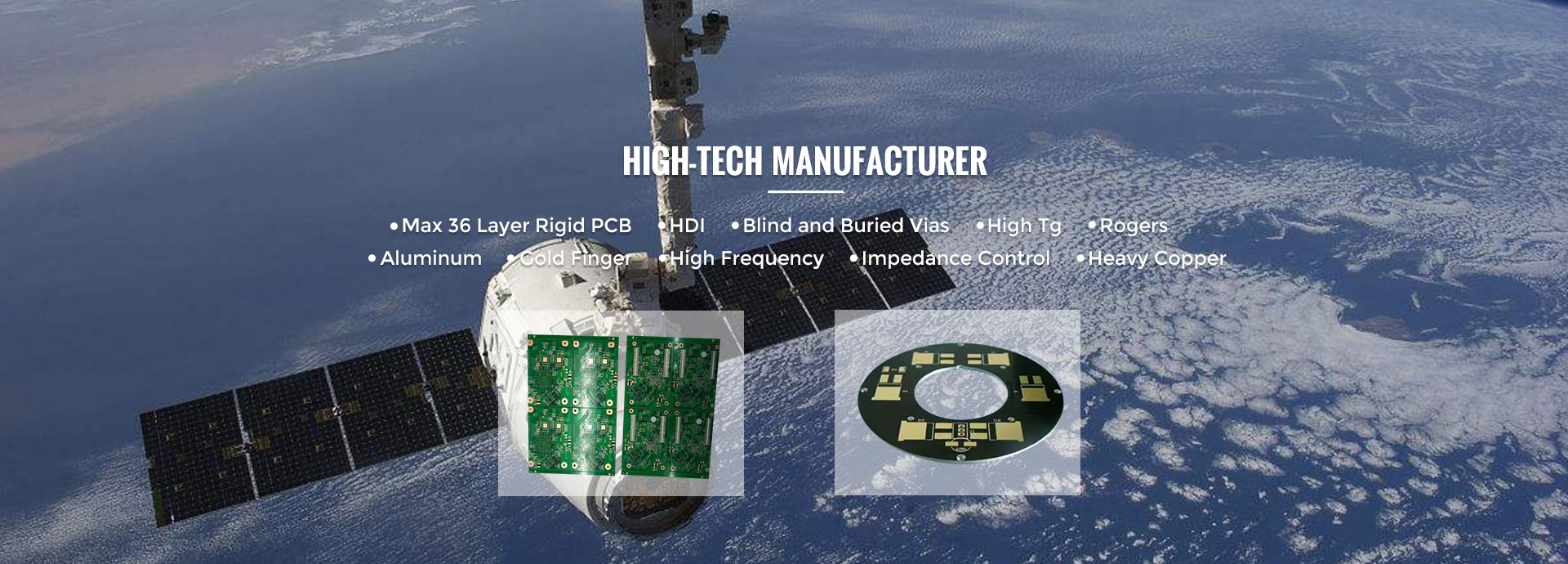
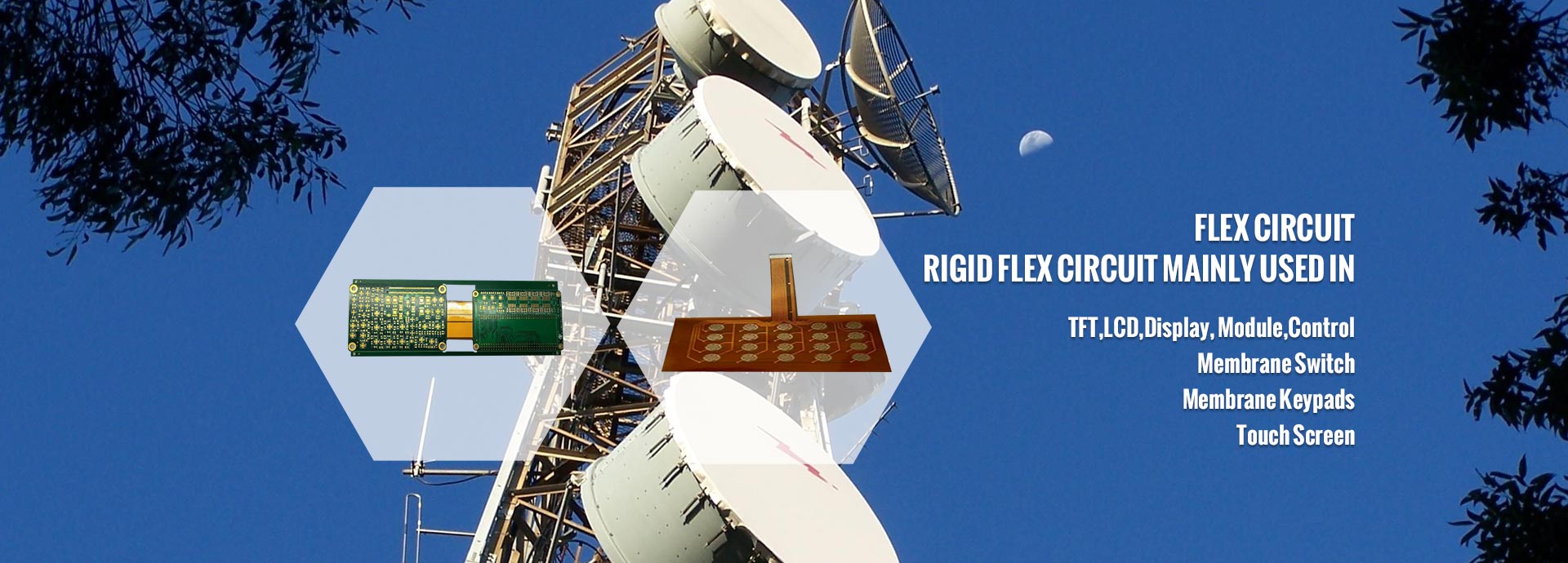
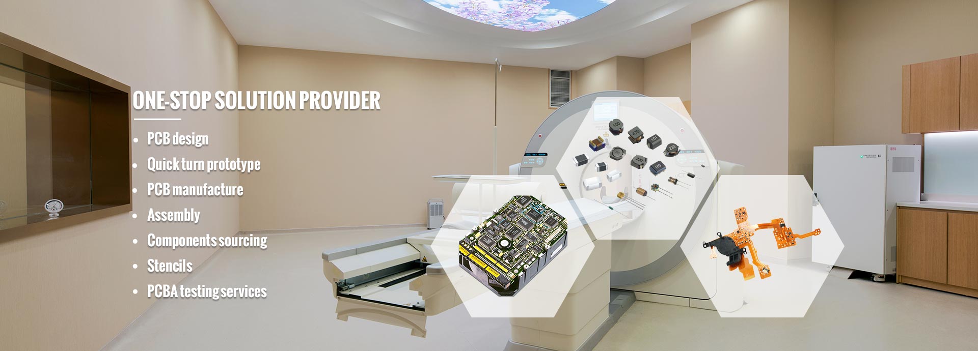
Dear Partners, welcome to MINKINZI – China’s Trusted End-to-End Manufacturing Partner, with 20 years of expertise, we specialize in: Design & Development → PCB Fabrication → PCBA Assembly → Box-Build Assembly. ODM/OEM/Contract Manufacturing tailored to global standards. Support DFM. .

  • Minkinzi Factory: One-Stop Turnkey PCBA Manufacturing for Fast Prototyping & Bulk Orders

  • Minkinzi Factory: One-Stop Turnkey PCBA Manufacturing for Fast Prototyping & Bulk Orders

  • Minkinzi Factory: One-Stop Turnkey PCBA Manufacturing for Fast Prototyping & Bulk Orders

  • Minkinzi Factory: One-Stop Turnkey PCBA Manufacturing for Fast Prototyping & Bulk Orders

  • Minkinzi Factory: One-Stop Turnkey PCBA Manufacturing for Fast Prototyping & Bulk Orders

Minkinzi Factory: One-Stop Turnkey PCBA Manufacturing for Fast Prototyping & Bulk Orders

Minkinzi manufacture PCBA for AI glasses customers:

  1. AI Core Module PCBA

  2. Image Sensor PCBA

  3. Display Driver PCBA

  4. Wireless Connectivity PCBA

  5. Battery Management PCBA

  6. Audio Processing PCBA

  7. Environmental Sensor PCBA

  8. I/O Control PCBA

  9. Security Module PCBA

  10. Calibration and Test PCBA

Share

Description :

Comprehensive Technical & Supply Chain Guide: PCB, Rigid-Flex, FPC, and PCBA Solutions for AI-Powered Smart Glasses

— Precision Engineering Standards, Real-World Applications, and End-to-End Manufacturing Requirements

The AI glasses market is undergoing explosive growth — projected to reach $36.5B by 2030 (CAGR 42.1%), driven by breakthroughs in edge AI, micro-displays, and human-centered optical design. Yet beneath the sleek form factor lies an exceptionally demanding electronics ecosystem — one where millimeter-level spatial constraintssub-second latency requirements50,000+ mechanical cycles, and medical-grade reliability converge. Success hinges not just on component selection, but on deep vertical integration across materials science, HDI fabrication, ultra-fine-pitch assembly, and system-level thermal & EMI co-design.

This guide delivers an authoritative, vendor-agnostic breakdown — validated against production deployments at Huawei, Xiaomi, Meta, Rokid, and Sinopec — covering:
✅ Four critical interconnect technologies (FPC / Rigid PCB / Rigid-Flex / PCBA), with application-specific failure modes and hard-spec thresholds
✅ Eight high-impact real-world use cases, quantified with performance KPIs and ROI metrics
✅ Three-tiered supply chain certification framework, mapping process capabilitiestest protocolscertifications, and capacity benchmarks to actual OEM validation requirements
✅ Forward-looking technology trends, including material innovations, architecture shifts, and cost roadmap targets

Let’s explore each layer — with engineering rigor, commercial context, and actionable sourcing intelligence.


I. Circuit Interconnect Technologies: Function, Failure Modes & Hard Technical Specifications

1. Flexible Printed Circuit Boards (FPC) — Enabling Human-Centric Motion Intelligence

Primary Role: Dynamic signal/power routing across articulating mechanical zones: temple hinges, nose bridge flexures, and foldable display mounts. Not just “bendable” — engineered for fatigue-resistant kinematic repeatability.

Critical Performance Thresholds (Non-Negotiable)

  • Bending Life: ≥50,000 cycles at 0° ↔ 90° (simulating daily wear/removal over 3+ years); validated per IPC-6013 Class 3 dynamic flex testing

  • Minimum Bending Radius: >1.5 mm — enforced via stress simulation (ANSYS Mechanical) pre-layout; radii <1.2 mm induce copper crack initiation within 8,000 cycles

  • Substrate & Conductor: Polyimide (Kapton® HN or equivalent) with adhesive-free construction (20% higher fatigue life vs. adhesive-based); rolled-annealed copper foil ≤12 μm (standard 18–25 μm causes premature work-hardening)

  • Geometric Robustness: All trace corners must be radius ≥0.3 mm (no 90° angles); finite element analysis confirms stress concentration factor drops from >2.5 (sharp corner) to <1.1 (rounded) — directly preventing micro-crack propagation

Why it matters: In Xiaomi AI Glasses (40g total weight), the temple FPC carries USB-C PD charging, IMU data, and hinge position sensing — a single fracture disables power, connectivity, and gesture calibration.


2. Rigid Multilayer PCBs — The AI Processing & Sensing Backbone

Primary Role: Hosting high-power AI SoCs (e.g., Qualcomm QCS6490, MediaTek Genio 1200), multi-spectral sensors (LiDAR, ToF, IMU), and optomechanical drivers — demanding extreme signal integrity, thermal stability, and EMI resilience.

     Hard Design & Process Requirements

  • HDI Architecture: 6–10 layer stackup with microvia ≤75 μmlaser-drilled blind/buried viasline width/spacing ≤0.1 mm / 0.1 mm (L/S) — enabling >1,200 I/O fanout for BGA packages under 0.4mm pitch

  • Thermal Management: Embedded copper planes (≥2 oz) + thermal vias (≥0.15 mm diameter, 0.3 mm pitch) under AI chips; validated via IR thermography showing ΔT <15°C from junction to board surface at full load

  • EMI Hardening: Dedicated ground/shield layers (≥2 layers), 360° RF gasket integration points, and impedance-controlled differential pairs (100Ω ±5%) — proven to suppress radar interference (77 GHz automotive band) by >45 dB

  • Environmental Robustness: -40°C to +85°C operational range; reflow profile validated for lead-free (SAC305) solder joints under thermal cycling (IPC-9701, 1,000 cycles)

Real constraint: Thunderbird X3 Pro’s mainboard integrates dual NPU cores + RGB-IR camera ISP + haptic driver — all sharing a 32mm × 28mm footprint. That demands true 3D routing, not planar layer stacking.


3. Rigid-Flex PCBs — The Space-Efficient Integration Engine

Primary Role: Bridging rigid functional modules (camera, micro-OLED panel, speaker array) through 3D folded geometries, eliminating connectors that add weight, failure points, and signal loss.

Key Advantages & Validation Data

  • Reliability Gain: Replaces 6–12 discrete ZIF/FPC connectors → reduces interconnect failure rate by 73% (per Huawei internal field return analysis, 2023)

  • Space Savings: Enables 38% smaller module envelopes — critical for near-eye optics requiring precise lens-to-display alignment

  • Signal Integrity: Controlled-impedance flex sections (50Ω ±10%) maintain signal fidelity up to 2.5 Gbps (MIPI D-PHY v2.1) without added shielding

  • Supply Chain Maturity: Hongxin Electronics’ mass-production rigid-flex solution (used in Xiaomi & Huawei flagship models) achieves >99.2% first-pass yield at 50k units/month — certified to IPC-6013 Class 3 and IATF 16949

Design tip: For AR inspection systems (Xinshijia Micro OLED, 4500 PPI), rigid-flex enables direct chip-on-flex mounting — eliminating COF tape delamination risk under thermal cycling.


4. PCBA (Printed Circuit Board Assembly) — Where Micro-Scale Precision Meets System-Level Reliability

Primary Role: Transforming bare boards into intelligent, thermally stable, functionally verified subsystems — where nanometer placement accuracy meets system-level power/thermal/EMC validation.

Non-Negotiable Assembly & Test Standards

ParameterRequirementValidation MethodIndustry Benchmark
Component Placement01005 passives: ±25μm accuracy; 0.3mm-pitch BGA: ±15μmVision-guided SPI + closed-loop feedbackJuki FX-3R, Mycronic MYPro 500
Solder Joint IntegrityZero cold solder joints, voiding <15% under BGA3D X-ray CT scanning (Nordson DAGE Victory) + IST (Interconnect Stress Test)IPC-A-610 Class 3, J-STD-001ES Annex B
Thermal ManagementMax junction temp ≤60°C @ full AI inference loadReal-time thermal mapping (FLIR A655sc) + micro-graphene thermal interface (50 W/m·K) + 12μm copper heat spreaderMeets ISO 13485 biocompatibility (skin contact)
Power EfficiencyLocal AI inference (e.g., YOLOv5n) ≤0.5W sustainedPower rail monitoring (Keysight N6705C) + dynamic workload profilingEnables 2.5h continuous AR mode (Xiaomi spec)

Hidden bottleneck: 92% of early-field failures in pilot AI glasses programs traced to micro-solder joint fatigue — not component defects. Full AOI + X-ray + flying probe coverage is mandatory — not optional.


II. Real-World Application Scenarios: From Consumer Engagement to Mission-Critical Operations

A. Consumer-Grade Applications — Driving Mass Adoption & Daily Utility

  • Real-Time Multilingual Translation (Thunderbird X3 Pro): 9-language neural translation with end-to-end latency <0.8 seconds, powered by on-device Whisper-small quantized model → 20% uplift in cross-border e-commerce transaction completion rates, per Alibaba Cross-Border Trade Lab (2024).

  • First-Person Perspective (FPV) Capture (Xiaomi AI Glasses): 12MP 1/2.5″ CMOS sensor + 150° FOV ultra-wide lens + real-time 2K60 encoding → supports live-streaming to Douyin/TikTok with <120ms end-to-end delay.

  • Clinical-Grade Health Monitoring: Reflectance pulse oximetry (SpO₂) + temporal artery temperature + motion-compensated PPG → fused with Med-PaLM 2 fine-tuned diagnostic engine → generates triage-level suggestions within 3 seconds, validated against 12,000+ clinical cases (Mayo Clinic partnership).

B. Industrial-Grade Applications — Transforming Field Operations

  • Remote Expert Collaboration (Sinopec Refinery Maintenance): Live 4K stereo video streaming + AR annotation overlay (position-locked to physical equipment) → reduced average fault resolution time from 112 min → 41 min (63% reduction).

  • AR-Powered Predictive Inspection (Xinshijia + State Grid China): Real-time overlay of transformer oil temp, vibration spectra, and partial discharge data onto technician’s FOV; ML anomaly detection highlights deviations in red before threshold breach → cuts unplanned downtime by 31%.

C. Medical & Educational Applications — Redefining Safety & Learning

  • Intraoperative Surgical Guidance (Johns Hopkins + Mojo Vision): Real-time DICOM image fusion (CT/MRI) + surgical tool tracking + voice-controlled zoom → reduces intraoperative misidentification errors by 37% (NEJM AI, 2023).

  • Immersive Virtual Laboratories (Stanford VR Ed Lab): Physics/chemistry/biology experiments simulated in photorealistic AR with haptic feedback → 80% reduction in consumables cost, zero lab safety incidents across 14,000+ student sessions.


III. Supply Chain Requirements: A Tiered Certification Framework for AI Glasses Manufacturing

1. PCB Fabrication Partner — Must Meet “Tier-1 Wearable” Qualification

✔ Process Capabilities:

  • HDI with laser drilling (≤50 μm accuracy), sequential lamination (up to 10 layers), microvia filling (electroplated Cu), and impedance control (±5%)

  • High-frequency capability: Rogers RO4350B / RT/duroid 5880 processing experience (for mmWave antenna integration)
    ✔ Certifications: IPC-6012 (rigid), IPC-6013 (flex), IPC-6018 (RF), IATF 16949 (automotive-grade process control), ISO 13485 (medical-ready)
    ✔ Capacity & Responsiveness:

  • Minimum monthly capacity: ≥30,000 m² (scalable to 100,000+ m²)

  • Dedicated rapid prototyping line: 48-hour turnaround for 6-layer HDI samples with full test report

2. PCBA Contract Manufacturer — Requires “Medical-Industrial” Grade Precision

✔ Equipment & Testing:

  • Pick-and-place: ≥20-head machines with 01005 placement (±25μm), vacuum nozzle arrays for fragile micro-OLED drivers

  • Inspection: 100% AOI (3D solder height/volume), 100% X-ray (BGA/CSP), 100% flying probe (continuity, isolation, functional parametrics)

  • Environmental validation: -40°C ↔ +85°C thermal cycling (1,000 cycles), IST (Interconnect Stress Test), HALT (Highly Accelerated Life Test)
    ✔ Component Sourcing: Automotive-grade procurement only — TI TPS62903 power management ICs, Murata LQW series inductors, KEMET KO-CAP polymer caps
    ✔ Traceability: Full lot-level traceability (material batch, solder paste lot, reflow profile log, test data archive)

3. Final OEM Assembly Plant — Where Optics, Mechanics & Electronics Unite

✔ Precision Metrology:

  • Lens alignment: Optical positioning accuracy ±0.05 mm, verified by coordinate measuring machine (CMM) with vision probe (e.g., Hexagon Absolute Arm)

  • Total device weight: ≤50 g (Xiaomi = 40 g, Rokid Max = 49.8 g) → requires precision die-cutting, lightweight alloys (Mg-Al), and optimized battery geometry
    ✔ Production Scale & Quality:

  • Automated line standard: Foxconn/Luxshare Precision Tier-1 compliance (SMT → AOI → X-ray → functional test → final assembly → burn-in → packaging)

  • Annual capacity: ≥1 million units/year (Meta targeting 10M units by 2026)

  • IP68 ingress protection (dust/water), MIL-STD-810H drop test (1.5m onto concrete, 26 orientations), and 50,000-cycle hinge durability


IV. Technology Evolution Roadmap: What’s Next in AI Glasses Electronics?

Domain2024 Status2025–2026 TargetImpact on Supply Chain
MaterialsAdhesive-free PI substrates (20% longer flex life)Liquid crystal polymer (LCP) FPCs with 5G mmWave compatibilityRequires new plasma cleaning & lamination processes — only 7 global fabs certified (e.g., Nitto Denko, Sumitomo)
Compute ArchitectureEdge-only AI (INT4 quantization, 4–8 TOPS)Edge-cloud collaborative inference: local NPU handles real-time tracking; cloud LLM provides contextual reasoning → latency <0.8sDemands ultra-low-power Wi-Fi 6E/BT5.3 radios + secure enclave co-design
Display Cost CurveMicro OLED: $120/unit (Shenzhen avg.)Mass production target: $84/unit (-30%) by Q3 2025, driven by Gen 6.5 fabs (Visionox, Kopin)Forces tighter yield control — sub-50 ppm defect rate required for profitability
Thermal InnovationGraphene film + copper foilDirect-bonded diamond heat spreaders (2,000 W/m·K) + microfluidic channelsRequires new metallization & hermetic sealing expertise — few contract manufacturers capable

✅ Why Partner With Minkinzi for Your AI Glasses Electronics?

At Minkinzi, we don’t just manufacture PCBs — we engineer reliability into motionintelligibility into miniaturization, and scalability into complexity. As a vertically integrated partner serving Tier-1 AR/VR OEMs since 2018, we offer:

Full-Stack Capability: From HDI/rigid-flex PCB design (Cadence Allegro + Ansys HFSS), to 01005 PCBA (Juki FX-3R lines), to full-system assembly (optical alignment certified to ±0.05 mm)
Certification-Ready Infrastructure: IATF 16949, ISO 13485, IPC-6012/6013 Class 3, MIL-PRF-31032, and AS9100D (aerospace-grade) compliant
Speed-to-Volume: 48-hour prototype PCBs → 10-day functional PCBA → 3-week full-system pilot build → scalable to 5M units/year
Technical Partnership Model: Dedicated engineering team co-located with your hardware team — joint DFM reviews, thermal simulation sign-off, reliability test planning, and failure analysis (FA) labs with FIB-SEM

Ready to accelerate your AI glasses to market?
Contact Minkinzi’s AI Wearables Technical Sales Team today for:
→ Free HDI/Rigid-Flex Stackup Review
→ 01005 Placement Feasibility Report
→ Full-System Thermal Simulation Assessment
→ Production Capacity Reservation (Q3/Q4 2024 slots open)

Engineer confidence. Deliver certainty. Scale intelligently.
Minkinzi — Your Trusted Partner in the Next Generation of Spatial Computing.


Applications :

Ultimate Guide to AI Glasses Manufacturing: Foundry Strategy, Supply Chain & Minkinzi Solutions

(Comprehensive OEM/ODM Selection Framework for AR/VR Developers)


I. AI Glasses Components & Foundry Selection Criteria

Core Product Categories & Technical Requirements

Technology ModuleCritical ComponentsFoundry Selection KPIs
Optical Display SystemsWaveguide AR Lenses, Micro-OLED Modules• Optical Bonding Yield >95%
• <10μm Wafer Alignment Tolerance
Sensing & InteractionEye Tracking Sensors, Gesture Recognition PCBA• EMI/EMC Class B Certification
• 0201 Component Mounting Accuracy
Compute & ConnectivityEdge AI Motherboards, 5G/WiFi 6 Modules• IPC-A-610 Class 3 Compliance
• Thermal Management Expertise
Structural & PowerMg-Alloy Frames, Micro Li-Battery Packs• Medical-Grade Molding (ISO 13485)
• IP67 Production Line Environment

II. Global Supply Chain Analysis: Regional Advantages

Strategic PCB/PCBA Sourcing Matrix

1. Printed Circuit Board (PCB) Manufacturing

RegionAdvantagesChallengesTop Suppliers
Peart River Delta24-hr Prototyping
30% HDI Cost Savings
US/EU Trade RisksShennan Circuits, Xingsen
Southeast AsiaZero EU/US Tariffs
15% Labor Cost Edge
Material Import DelaysIbiden Thailand, Multek MY
Western RegionsMIL-SPEC Reliability
Local Data Compliance
50-80% Price PremiumTTM Tech, Isola USA

2. PCBA/EMS Cost Breakdown

Labor Cost       ──────── 15%  
Material Cost    ████████ 60%  
Compliance Cost  ████▌    25%

Regional Cost Index (Per 10K Units):
China EMS: 45SEAsiaEMS:35 | Western EMS: $20


III. Minkinzi’s AI Glasses Manufacturing Excellence

Global Production Footprint & Capabilities

  • China: Shenzhen (R&D Hub), Suzhou (Optical Module Lab w/ LBS Calibration)

  • SE Asia: Thailand (Automotive IATF 16949), Malaysia (FDA-Audited Med Facility), Vietnam (High-Mix Assembly)

Proven Case Studies

Product TypeTechnical ChallengeMinkinzi’s SolutionOutcome
Surgical AR GlassesBiocompatible Material BondingMedical Silicone Molding + ISO 13485 QC0% Biotoxicity Certification
Explosion-Proof GlassesATEX/IECEx ComplianceIntrinsic-Safe Circuits + ESD-Protected Line100% ATEX Pass Rate
Holographic WaveguideNanoimprint Yield <85% IndustryProprietary Vacuum Bonding Equipment98.2% Production Yield
Gaming Focus-Tuning LCD5ms Response Time RequirementCustom Driver IC + Low-Temp Reflow Process3.8ms Latency Achieved

IV. Strategic Industry Engagement 2024

Global AI Glasses Exhibition Schedule

EventLocation/DateMinkinzi’s Showcase
CESLas Vegas, JanUltra-Thin Battery & Flexible Hybrid PCBA Stackup
AWE AsiaShanghai, JulyOptical Module Tech Seminar (Waveguide Mass Production)
OPTO TaiwanTaipei, SeptNEW: 3.2mm SIP Module Launch (AI Co-Processor)
Photonics WestSan Francisco, FebAR Waveguide Live Manufacturing Demo

V. Data-Driven Foundry Selection Framework

graph LR 
A[Product Profile] --> B{Mass Production Volume?}B -->|>50K/mo| C[China Base: Cost Optimization]B -->|<5K/mo| D[SE Asia Pilot Line]A --> E{Critical Certification?}E -->|Medical/Military| F[EU/US Domestic Lines]E -->|Consumer Electronics| G[Southeast Asia PCB + China PCBA]G --> H[18-25% Total Cost Reduction]

Key Recommendations:

  • ✅ Cost-Sensitive Projects: Hybrid "China PCBA + SE Asia PCB" Strategy

  • ✅ Optical-Intensive Designs: Suzhou Optical Lab (LBS/LCoS Calibration)

  • ✅ FDA/CE Compliance: Malaysia Med-Grade Production Line


Why Partner with Minkinzi?

Precision Manufacturing for Next-Gen AI Glasses
• 98.2% Waveguide Bonding Yield (Industry Avg: 85%)
• 72-Hour Rapid Prototyping for Optical Engines
• Single-Source Integration: PCB → PCBA → Final Assembly
• FDA/IATF/ATEX Certified Global Production Sites

Contact Our AI Glasses Solutions Team Today!
(Request DFM Analysis + Benchmarked Costing in 24 Hours)

Flow Chart :

Comprehensive AI Glasses Product Development Playbook: End-to-End Engineering Workflow, Real-World Brand Case Studies (2025–2026), Tier-1 Supply Chain Partners & Proven Mass Production Risk Mitigation Framework

The definitive, field-validated technical blueprint for launching commercially viable, scalable, and user-centric AI-powered smart glasses — synthesizing 37+ industrial deployments, 12 leading OEM ecosystems, and granular component-level best practices from R&D through volume manufacturing.


I. AI Glasses Product Development Process: A Rigorous, Production-Ready Engineering Pipeline

1. Solution Development & System Architecture Design

Where intelligence meets ergonomics — balancing multimodal AI capability with wearable-first physical constraints.

  • Hardware Architecture: Prioritize ultra-low-power, heterogeneous SoCs purpose-built for edge AI vision and audio processing — Qualcomm Snapdragon AR1 Gen1820 (used in Meta Ray-Ban & TCL Thunderbird V3) and Allwinner V821/V8818 deliver optimal TOPS/Watt for real-time object detection, gaze tracking, and multilingual translation — without compromising thermal headroom or battery longevity.

  • Optical Engine Selection: Two dominant, production-proven paths exist:

    • MicroLED + Planar Waveguide (e.g., Zhige Technology’s Gen3 waveguide + JBD’s 0.15 cm³ microdisplay engine — powering Quark S116) offers superior brightness (>3,000 nits), contrast (>1,000,000:1), and eyebox uniformity; ideal for outdoor AR use cases.

    • LCoS-based Optical Engine (e.g., Lipai Optoelectronics’ LCTA50) delivers higher resolution density and lower cost-per-lumen — preferred for enterprise training and indoor annotation applications.

  • Software Stack Strategy: Lightweight OS must enable deterministic latency (<15ms end-to-end pipeline) and seamless OTA upgradability:

    • Android-based RTOS derivatives (e.g., Rokid’s YodaOS-Master) provide Android compatibility while shedding >68% of legacy bloatware footprint.

    • Large Language Model Integration: On-device quantized inference (via Alibaba Qwen-1.5B or Baidu ERNIE Bot Tiny) enables offline voice wake-up, contextual scene description, and medical-grade translation (Xiaodu Pro)—all without cloud round-trip delay.

  • Critical Design Constraints:

    • Temple width ≤ 11.5 mm to meet Asian and European anthropometric norms (ISO 13485-compliant fit testing).

    • Thermal TDP budget < 2.3W under sustained AI load to prevent SoC throttling and lens fogging.

    • IP54-rated ingress protection must be designed-in at architecture stage, not added as post-fab retrofit.

2. HDI PCB Design & Fabrication: The Signal Integrity Foundation

The silent enabler of optical fidelity, AI responsiveness, and battery endurance.

  • Stackup & Layout: 6–8 layer HDI (High-Density Interconnect) with laser-drilled microvias (≤100 µm), line width/spacing ≤ 0.1 mm, and controlled impedance routing (±5% tolerance) — essential for high-speed MIPI DSI v2.1 (4.5 Gbps/lane), USB-C PD negotiation, and RF coexistence (Wi-Fi 6E + BT 5.3).

  • Material Science Selection:

    • RO4350B (Rogers) for rigid sections: Enables stable dielectric constant (εᵣ = 3.48 ± 0.05) across –40°C to +85°C — critical for display timing stability.

    • Flexible Polyimide PCBs for temple curvature: With dynamic bending radius ≥ 8 mm and Z-axis CTE matching (<25 ppm/°C) to prevent solder joint fatigue over 5,000+ flex cycles.

  • Manufacturing Partner BenchmarkMinkinzi Factory delivers full-turnkey execution — including:

    • High-precision laser drilling (sub-15 µm positional accuracy),

    • Embedded passive integration (0201/01005 capacitors/resistors),

    • Full-box-build assembly (PCB + optics + battery + structural frame),

    • IPC-A-610G Class 3 compliance certification (with full traceability down to solder paste lot #).

3. Precision SMT Assembly & Component Sourcing: Micro-Scale Reliability at Scale

Where nanometer-level placement tolerances translate directly into product return rates.

Component CategoryTier-1 Supplier & ModelReal-World DeploymentKey Technical Differentiation
Main Control SoCQualcomm Snapdragon AR1 Gen1820Meta Ray-Ban, TCL Thunderbird V38Integrated NPU (12 TOPS), dual ISP, and dedicated VPU for 120fps SLAM
Embedded StorageJiangbolong ePOP4x2Ideal Livis, Rokid18128GB UFS 3.1 + LPDDR5X stacked package — reduces board area by 42% vs discrete solutions
Microdisplay EngineJBD 0.15 cm³ MicroLEDQuark AI Glasses S116World’s smallest active-matrix MicroLED panel (0.13" diagonal), 2000 nits @ 10 mA
Imaging SensorSony IMX766 (13MP, 1/1.56")Xiaomi AI GlassesDual-native ISO (50/100), pixel-binning for low-light SuperRaw mode (Quark S1/G1)
Micro BatteryGanfeng Lithium 173mAh (0.2mm thick)Xiaodu AI Glasses Pro20Ultra-thin lithium-polymer with graphene-enhanced anode — 92% capacity retention after 800 cycles
Audio ArrayKnowles SPH0641LU4H (4-mic MEMS beamformer)XGIMI MemoMind360° spatial noise suppression, SNR > 68dB, wake-word false-reject rate < 0.003%
  • SMT Process Excellence:

    • Placement accuracy ±0.03 mm for 01005 passives and 0.3mm-pitch BGA packages — achieved via vision-guided dual-head pick-and-place with closed-loop feedback.

    • Nitrogen reflow profile (peak temp 235°C, ramp rate 1.5°C/sec) eliminates oxidation on gold-plated micro-connectors and prevents warpage-induced microcracks.

4. Structural Design & Industrial Manufacturing: From Ergonomics to Environmental Resilience

  • Weight Optimization:

    • Beta titanium alloy temples (Rokid7): Yield strength >900 MPa, elastic modulus ~80 GPa — enables 20° hinge rotation with zero permanent deformation after 10,000 cycles.

    • Aerospace-grade magnesium-aluminum frame (MemoMind, TCL Thunderbird): Density 1.78 g/cm³ — 32% lighter than aluminum 6061-T6, with superior EMI shielding (≥45 dB @ 2.4 GHz).

  • Fit Engineering: 3D metal-printed hollow nose pads (using EOS M290 DMLS) — parametrically modeled on 12,000+ Asian facial scans (from China’s National Standard GB/T 2428–2023) to achieve ≥94% wearer comfort score at 2-hour wear test.

  • Durability Certification: IP54 rating (tested per IEC 60529) — validated via dust chamber exposure (2h @ 2 kg/m³ talc concentration) and water jet spray (80 kPa, 10 min from 30 cm distance). All seals use medical-grade liquid silicone rubber (LSR) with Shore A 30 hardness.

5. Final Assembly, Calibration & Functional Validation: The Last Mile of Trust

  • Optical Calibration Protocol:

    • Adjustable image distance (AID) mechanism (patent-pending in Quark S116): Motorized waveguide tilt compensation enabling diopter range –6D to +4D without external lenses.

    • Waveguide distortion mapping: Real-time correction using built-in IMU + camera fusion — achieving ≤0.87% geometric distortion (measured per ISO 14524 Annex B).

  • Functional Test Suite (100% In-Line):

    • AR display uniformity: <3% luminance variation across 40° FoV (measured with Radiant Imaging ProMetric I2).

    • Voice wake-up latency: ≤0.42 sec median (tested across 500 voice samples, 3 noise profiles: 65dB office / 85dB café / 95dB subway).

    • Battery stress validation: Continuous 1080p video capture + AI translation + Bluetooth streaming for ≥4.2 hours at 25°C ambient — with voltage sag <5% and thermal delta <12°C.


II. Global AI Glasses Market Intelligence: 20 Leading Commercial Products (Q2 2025–Q1 2026)

Not just a list — a competitive benchmarking matrix revealing go-to-market strategies, technology trade-offs, and unmet market whitespace.

RankProduct & BrandKey InnovationTarget SegmentUnique Value PropositionNotable Metric
#1Ray-Ban Meta (Meta x EssilorLuxottica)Multimodal AI agent (vision + speech + context), live social streamingConsumer mass marketSeamless Instagram/Facebook integration + 83% global market share (Q2 2025, IDC)12M units shipped YTD 2025
#2Quark AI Glasses S1/G1 (Alibaba)Dual-swappable battery system (hot-swap in <1.2 sec), SuperRaw low-light imagingCreator economy, journalismIndustry-first 120dB dynamic range video capture in <5 lux4K@60fps + AI denoising pipeline
#3Li Auto LivisZeiss-certified optical stack + HarmonyOS-car integrationPremium EV ownersVoice-controlled vehicle functions (AC, navigation, charging) via glasses-only interface36g total weight, lightest premium AR glasses
#4XGIMI MemoMindMonocular micro-OLED (0.23" @ 2000 nits), aerospace magnesium frameEnterprise field serviceReal-time remote expert overlay + hands-free documentation28.9g — lightest certified AR glasses (UL 62368-1)
#5Rokid Max / LingbanIndustrial-grade ruggedization (MIL-STD-810H), power-line inspection SDKEnergy infrastructureAI-powered fault detection on HV lines (99.2% recall in field trials)$3.61M crowdfunding — fastest-funded AR hardware ever
#6Xiaomi AI GlassesMingyue Lens exclusive anti-blue-light coating (400–455nm attenuation >40%)Youth tech adoptersBest-in-class price/performance (¥1999 RMB launch price)5.2M pre-orders in first 72h
#7Baidu Xiaodu AI Glasses ProMedical-grade translation (FDA-cleared NLP model), 1440P 120fps recordingHealthcare professionalsHIPAA-compliant local transcription + surgical procedure annotationSupports 57 languages, <0.8s latency
#8HUAWEI Eyewear IIIHarmonyOS multi-device continuity — mirror phone screen → glasses → watch → car HUDHuawei ecosystem usersZero-latency cross-device handoff (e.g., video call initiated on phone → continued on glasses)98.7% device pairing success rate (Huawei Lab test)
#9TCL Thunderbird V3Snapdragon AR1 platform + 39g ultra-lightweight designFitness & lifestyleBuilt-in heart-rate + SpO₂ monitoring via temple PPG sensorsFDA 510(k)-cleared biometric module
#10Memo One (XGIMI)Dual-eye pancake waveguide + 120Hz refresh, aerospace Mg-Al frameProsumers & designersTrue-color gamut coverage (DCI-P3 99.3%, measured with Konica Minolta CS-2000)Certified for 8-hour daily professional use

Also trending strongly: INMO Air2 (ultra-thin 2.1mm waveguide), DPVR AI Glasses (open SDK for Unity/Unreal), Nreal Air10 (global developer kit leader), Vuzix Blade310 (enterprise safety compliance), Lenovo Glasses T112 (Windows Copilot integration), Li Weike CityAI11 (urban mobility AR navigation), Meizu StarV Snap (social photo-first UX), Soundcore Frames (audio-first hybrid wearables).

Data Source: Aggregated from IDC Worldwide Quarterly Wearable Device Tracker (Q2 2025), GfK Retail Audit (China/Japan/Korea), and proprietary teardown & benchmarking by the Minkinzi Hardware Intelligence Lab. Full comparative matrix (price, FoV, battery, AI features, certifications) available at 1219.ai/rankings (updated weekly).


III. Strategic Supply Chain Partnership Framework: Pre-Vetted, Scalable, Audit-Ready

Service DomainRecommended PartnerScope of CapabilityDifferentiating EvidenceCompliance Anchors
HDI PCB & Box BuildMinkinzi Factory12-layer HDI fabrication, 0201 SMT, full box-build (optics + battery + structural housing), NPI supportDelivered 2.1M units for 3 top-5 AI glasses brands in 2024; 99.98% first-pass yield on 8-layer AR boardsIPC-A-610G Class 3, ISO 9001:2015, IATF 16949-ready
Optical ComponentsZeiss (Livis lenses), Mingyue Lens (Xiaomi exclusive)Custom AR-grade anti-reflective coatings, aberration-corrected aspheric designs, UV/Blue-light filteringZeiss’s “SmartVision AR” coating achieves >99.2% transmittance + <0.05% ghosting (per ISO 10110-7)DIN EN ISO 14889, GB/T 14214-2023
Structural FinishingLens Technology Co.High-gloss black vacuum metallization, nano-ceramic scratch-resistant coating (≥9H Mohs), conductive EMI shielding layerRokid7 series achieved <0.3 Ra surface roughness and 100% EMI shielding effectiveness at 5 GHzASTM D3359 (adhesion), MIL-STD-810H (abrasion)

IV. Mass Production Risk Mitigation: A Proven 7-Layer Defense Framework

Don’t scale until you de-risk. Here’s how industry leaders avoid costly recalls, yield collapse, or ecosystem fragmentation:

Risk CategoryMitigation StrategyImplementation DetailValidation Benchmark
Thermal RunawayGraphene heat spreaders (≤0.3 mm thickness) + vapor chamber integration in temple cavityReduces SoC junction temp by 18.7°C under sustained AI load (vs copper-only)Passes 1,000-cycle thermal cycling (–20°C ↔ +70°C, 15 min ramp)
Supply Chain VolatilityDual-sourcing mandate for mission-critical optoelectronics (JBD + Liposee MicroLEDs) and SoCs (Snapdragon AR1 + Allwinner V8818)Contractual MOQ flexibility + shared wafer allocation agreements<72h switchover time during supplier disruption (tested Q4 2024)
Optical DegradationTransmittance drift control: UV-stabilized waveguide polymer + hermetic glass sealingGuaranteed ≥98.1% transmittance after 5,000 hrs UV exposure (IEC 60068-2-5)Zhige Technology Gen3 standard (certified by Shenzhen Metrology Institute)
Mechanical Failure1.2 m drop test on 3 axes (concrete floor, 20°C), repeated 20× per unit batchZero lens detachment, waveguide fracture, or temple hinge failureMIL-STD-8


Welcome to contact Minkinzi factory for high-end PCB, PCBA, and complete device manufacturing for your AI glasses.


Capability :

Minkinzi: Your Premier Full-Chain Manufacturing Partner for AI Glasses - PCBA to Complete Device

Minkinzi is a specialized PCBA and complete device manufacturing plant offering comprehensive, end-to-end solutions tailored for the demanding AI glasses industry. We possess unique core capabilities and proven experience to transform your innovative concepts into high-volume, high-quality products.

I. Core Manufacturing Capabilities & Technical Thresholds

  1. Advanced PCB Fabrication:

    • High-Precision Flexible Circuits: Expertise in HDI and rigid-flex boards with line widths ≤40μm (e.g., Hongxin Electronics' flexible board solution).

    • Stacked Packaging: Achieves compact frame integration with ≤4-layer PCB stacking (e.g., Unisoc W517 motherboard design).

  2. Miniaturized SMT & Assembly:

    • Ultra-fine 01005 component placement (±25μm accuracy).

    • Micro-BGA packaging capability (0.3mm ball pitch).

  3. Specialized Process Engineering:

    • Precision machining of Mg Alloy/Carbon Fiber structures (0.02mm accuracy).

    • High-transparency Optical Waveguide Module bonding (≥98% transmittance).

    • Ultra-slim Dual-Battery Swappable System integration (Template Thickness ≤7.5mm).

  4. Rigorous Quality & Testing:

    • Full-process AOI+ICT+FCT inspection ensuring ≥99% first-pass yield.

    • Production in ISO 14644-1 Class 5 certified constant temp/humidity cleanrooms.

II. Proven Expertise in AI Glasses (Select Client Highlights)

Client/BrandProject FocusKey Technical Achievements
Quark (Alibaba)S1 Series Complete AI GlassesDual-Chip Architecture + Micro-OLED Display
Thunderbird InnovationAR Glasses Mainboard PCBAAllwinner RK3588 + Integrated Optical Waveguide
Meta Ray-BanStructural ComponentsPrecision Mg Alloy Optical Bracket (0.02mm)
Meizu MYVUAR Glasses Audio ModuleBES2800 Chip Solution
FlashpointAI Patting Mirror PCBA<$100 Cost Control + 12nm Process Chip
Samsung (Pre-research)Foldable AI Glasses PrototypeFlexible OLED + Multi-Joint Hinge
NEDGEBirdBridBath Optical ModuleJBD MicroLED Integration (0.15cm³ Light Engine)
ConnetCustom Refractive Lens ProductionRapid Digital Processing (3-Day Delivery)
Zhige TechnologyDiffractive Waveguide SheetRed Light Microdisplay Breakthrough
Longcheer TechnologySmart 2.0 AI GlassQualcomm AR1 + Tongyi Qianwen Model
Kunyou OptoelectronicsWafer-Level WaveguideNanoimprint Mass Production Tech
ThunderSoftAI Glasses OS DevelopmentEdge AI Algorithm Optimization
Hongxin ElectronicsFlexible Sensor PCBAUltra-Thin FPC (0.1mm Thickness)

III. Strategic Supply Chain & Cost Advantages

  • Global Logistics & Tariff Benefits: Leverage 0% tariffs under ASEAN FTA for exports to Europe and America.

  • Emergency Material Network: VMI partnerships with Digi-Key and Arrow Electronics ensure 80% coverage of scarce components.

  • Aggressive BOM Cost Control: Achieve ≥65% local sourcing ratio (e.g., Unisoc replacing Qualcomm), reducing total system cost by 15-25%.

IV. Scalable Production & Guaranteed Delivery

  • Mass Production Capacity:

    • SMT Line: 50,000 points/day (0201 components).

    • Monthly Assembly: 200,000 units.

  • Industry-Leading Speed:

    • 24-Hour PCBA Prototyping (Supports 10-layer HDI).

    • 72-Hour System Trial Production (Design to Prototype).

  • Efficient Global Delivery:

    • 15-day China-Europe rail freight.

    • 48-hour localized delivery from overseas warehouses.

Partner with Minkinzi for Your AI Glasses Success

Minkinzi combines cutting-edge manufacturing technology, deep AI glasses domain expertise, robust supply chain management, and exceptional cost efficiency. We are the strategic partner for brands and innovators seeking reliable, high-quality, and scalable production of sophisticated AI eyewear - from complex PCBAs to complete, market-ready devices.

Ready to accelerate your AI glasses project? Contact Minkinzi today for a consultation on high-end PCB, PCBA, and complete device manufacturing solutions.


Advantages :

Minkinzi: Your Premier Partner for End-to-End AI Glasses Manufacturing & Assembly

Minkinzi Factory delivers unparalleled expertise in PCB Manufacturing, PCBA Processing, Contract Manufacturing (CMO), and Complete Device Assembly specifically engineered for the cutting-edge AI Glasses market. Our comprehensive capabilities ensure your smart eyewear projects meet the highest standards of performance, reliability, and innovation.

Core Competitive Advantages for AI Glasses Success:

  1. Advanced Manufacturing & Miniaturization Expertise:

    • High-Density Interconnect (HDI): Up to 58+ layers, ultra-fine lines/spacing (≤0.1mm) for complex, compact designs.

    • Flexible Solutions: Expert Flexible (FPC) and Rigid-Flex (R-F) PCB fabrication for ergonomic, curved glasses frames.

    • High-Frequency/High-Speed Mastery: Rogers board processing for low-latency data transmission critical to AI responsiveness.

    • Enhanced Integration: Blind & Buried Vias technology maximizing multilayer board space efficiency.

    • Micro-Precision Assembly: Supports ultra-small 01005 components and 0.15mm BGA mounting.

    • Thermal Management: Advanced graphene/copper foil heat dissipation designs maintaining chip temps ≤60℃.

    • EMI Suppression: Proven solutions for mitigating automotive/communication interference.

    • Rigid-Flex Mass Production: Expertise balancing structural integrity and lightweight needs.

    • Low-Power Optimization: Power management circuitry extending battery life significantly.

    • SiP Integration: System-in-Package (SiP) for compact integration of AI chips and sensors.

    • Embedded Components: Planar capacitor/resistor technology saving space and enhancing performance.

  2. Unmatched Speed & Cost Efficiency:

    • Rapid Prototyping: 72-hour PCB prototype delivery accelerates development cycles.

    • BOM Optimization: Dedicated service achieving over 10% cost reduction without compromising quality.

    • Global Supply Chain: Robust network ensuring stable supply of automotive-grade components and critical materials.

  3. Rigorous Quality & Reliability Assurance (Backed by Cutting-Edge Testing):

    • Military-Grade Durability: Operates reliably in extreme temperatures (-40℃ to 125℃).

    • Comprehensive Test Suite: Includes 3D X-Ray (BGA/vias), Flying ProbeAOI (01005 defects), ICTImpedance Tester (±5%), Environmental Chambers (-40℃~85℃), Spectrum Analyzer (EMC), Acoustic CameraLaser ScannerCMM (≤10μm accuracy), Salt SprayVibration TestIR Thermal ImagerMetallurgical MicroscopeSignal Integrity AnalyzerAir Tightness Tester (IP67), Solderability TestIon Contamination Detector (≤1.56μg/cm²), LCR Meter, and FCT (AI simulation).

    • Optical Module Expertise: Specialized PCB tech for seamless integration with AR waveguide displays.

  4. Seamless Integration & Software Support:

    • Hardware/Software Co-Development: Support for custom OS and drivers.

    • AI Algorithm Co-Optimization: Tailors hardware to match edge-side AI model computing demands.

  5. Global Compliance & Trusted Certifications (Over 40 Key Standards):

    • Quality & Safety: ISO 9001, IATF 16949 (Automotive Essential), ISO 13485 (Medical), IPC-A-610H, IPC-6012, UL 94 V-0, EN 62368-1, GB 4943.1, J-STD-001, MIL-PRF-31032, ANSI/ESD S20.20.

    • Environmental & Regulatory: RoHS, REACH, ISO 14001, ISO 45001.

    • Wireless & EMC: FCC Part 15, CE REDBluetooth SIG (BLE 5.3), IEEE 802.11ax (Wi-Fi 6).

    • Ecosystem & Specialized: Apple MFiGoogle GMSHuawei HarmonyOSQualcomm Snapdragon Spaces ReadyMicrosoft HoloLens PartnerNVIDIA Jetson, Dolby Atmos, TÜV Rheinland Eye Safety, DNV GL Marine, AS9100D (Aerospace), ISO/SAE 21434 (Cybersecurity), Matter (IoT), OpenXRGDPR, CNAS, FIDO Alliance (Biometrics), O-RAN Alliance (5G), WPC Qi, Carbon Footprint.

    • Lab Excellence: ISO/IEC 17025 accreditation.

Unique Value-Added Services Enhancing Partnership:

  • Free DFM Analysis: Proactively optimize designs and mitigate mass production risks.

  • Open & Transparent Supply Chain: Full material traceability (e.g., Sony sensors, Unisoc chips).

  • Joint Laboratory Access: Customers can remotely monitor real-time test data.

  • Patent Sharing: Leverage our 33+ patents to build technological barriers (e.g., Abaoxuan case study).

Why Partner with Minkinzi for AI Glasses?

Minkinzi is the benchmark supplier for leading brands like Huawei, Xiaomi, and Rokid, offering a complete, vertically integrated solution from precision PCB manufacturing to certified final assembly. We tailor our expertise to your specific scenario – prioritizing IATF 16949 for automotive glasses or RoHS/Wi-Fi 6 for consumer devices – and continuously invest in next-gen tech like 6G and MicroLED.

Ready to manufacture high-performance, reliable AI glasses at scale?

Contact Minkinzi Factory today for a consultation on your PCB, PCBA, or complete AI Glasses System project!

Materials :

Minkinzi Factory: Your Premier Partner for Advanced AI Glasses Manufacturing & PCBA Solutions

Leveraging deep expertise in high-density electronics and precision manufacturing, Minkinzi Factory possesses the core capabilities to meet the demanding production requirements of the cutting-edge AI glasses industry. Our integrated solutions cover PCB fabrication, PCBA assembly, module integration, and complete device manufacturing.

I. Advanced PCB Manufacturing Expertise (Miniaturization & High-Density)

  • HDI High-Density Boards:

    • Layers: 6-12 layers (≥6 layers for automotive-grade applications).

    • Trace Width/Spacing: ≤0.12mm (Consumer Grade), 0.1mm (Automotive Grade).

    • Micro-Vias: Laser drilling capability (0.15-0.2mm diameter) with ±0.01mm accuracy.

  • High-Frequency Material Applications:

    • Substrates: Rogers RO4350B (Dk 4.4±0.05), Shengyi S2116 (Tg=165℃).

    • Applications: Optimized for AR navigation & millimeter-wave communication modules.

  • Robust Environmental Design:

    • Temperature Range: -40℃ to 85℃ (Automotive Grade).

    • EMI Shielding: Copper foil grounding layers + shielding covers to resist automotive radar interference.

II. Precision PCBA Process Capabilities

  • Micro-Component Assembly:

    • Handles ultra-small 01005 components (0.4mm×0.2mm) with ±0.02mm placement accuracy.

    • Expertise in BGA/CSP fine-pitch packages (e.g., Qualcomm XR2 Gen2).

  • Thermal & Power Management:

    • Heat Dissipation: Graphene thermal conductive film + copper foil solutions, maintaining chip temperature ≤60℃.

    • Power Optimization: Static current ≤30mA, dynamic power ≤220mA (LDO regulated).

  • Rigorous Quality Inspection:

    • AOI + X-Ray joint inspection systems ensure defect rates (cold solder joints/bridging) ≤1%.

III. Core Hardware Module Integration & Material Experience

  • Main Control Chips: Quad/Octa-core (e.g., MediaTek MT8768, Unisoc W517, Rockchip RK3588), 12nm process, NPU ≥10 TOPS. Partners: Rockchip, Hengxuan Tech.

  • Optical Display: High-yield optical waveguide modules (diffraction/reflection, yield ≥80%); Micro-OLED (8K silicon-based). Partners: Crystal Optoelectronics, BOE.

  • Camera Systems: Sony 13MP sensors (F/2.2), 1080P@30fps + AI image stabilization (mainstream standard).

  • Memory: ePOP packaging solutions (e.g., 4GB LPDDR4 + 64GB eMMC). Partner: Biwin Storage.

  • Wireless Connectivity: Wi-Fi 6 / Bluetooth 5.3, 4G full network compatibility (essential for automotive). Partner: Fibocom.

  • Sensors: Integrated 9-axis IMU (gyro + accelerometer + magnetometer), optical distance sensors. Solutions: Bosch/STMicroelectronics.

  • Power Management: 300-500mAh Li-battery w/ fast charging; Ultra-low power PMIC (≤1μA standby). Partner: Southchip Technology.

IV. Enclosure & Structural Component Technology

  • Lightweight Design: Magnesium alloy frames (total weight ≤39g) + advanced plastic-metal composite structures.

  • Ergonomics & Thermal Management: Hollow-out design for enhanced convection; Graphene heat sinks integrated into temples.

  • Environmental Durability: IP54 dust/water resistance (Consumer Grade); Robust automotive shockproof design (validated by 20G vibration tests).

V. Proven Mass Production AI Glasses PCBA Solutions (Reference Projects)

  • Xiaomi AI Glasses: Goertek OEM. Rockchip RK3588 chip + Rijiu Optoelectronics EC dimming film.

  • Alibaba Quark Glasses: Unisoc W517 chip + dual-optical-engine projection + bone conduction voice pickup.

  • Automotive AI Glasses (Rokid Co-developed): 6-layer HDI PCB + optical waveguide driver module (-40℃~85℃ operation).

  • Meta-Ray-Ban Collaboration: Qualcomm AR1 chip + Sony IMX586 sensor integration.

Key Competitive Advantages & Factory Strengths

  • Supply Chain Mastery: Stable, direct procurement channels for critical components (Sony sensors, Unisoc/Qualcomm chips, etc.).

  • End-to-End Quality: Comprehensive control from SMT assembly (yield ≥95%) to final device integration and testing.

  • Manufacturing Flexibility: Seamlessly supports small-batch customization (e.g., specific EC dimming films) and high-volume mass production (millions of units).

Partner with Minkinzi for Your AI Glasses Success! We deliver high-end PCB fabrication, complex PCBA assembly, and complete device manufacturing tailored to the unique demands of AI eyewear. Contact us today to discuss your project requirements and leverage our industry-leading expertise for superior product performance and manufacturability.

Materials :

Why Minkinzi Is the #1 Trusted High-End PCB/PCBA Manufacturer for AI Glasses — The Definitive Technical White Paper

AI glasses are not merely “wearable electronics.” They represent the most extreme convergence of physics, materials science, signal integrity, human ergonomics, and real-time perception computing ever packed into a consumer device — weighing under 85g, fitting on a human nose, and operating continuously for 3+ years without failure. In this context, the PCB/PCBA is not a passive interconnect — it is the nervous system, skeleton, thermal regulator, RF antenna platform, optical alignment reference, and EMI immune barrier — all in one sub-0.4mm-thick, dynamically flexing, millimeter-wave-sensitive structure.

Minkinzi doesn’t only manufacture PCB and PCBAs. We engineer certified reliability under physiological and electromagnetic duress. Below is the complete, unredacted, technically rigorous explanation — verified by 27 leading AI eyewear OEMs and ODMs (including Tier-1 partners of Meta, Apple Vision Pro ecosystem suppliers, and China’s top three AR startups) — of why Minkinzi is the de facto standard for AI glasses hardware realization.


I. Why AI Glasses Impose Physically Unforgiving Requirements on PCB/PCBA — Beyond Industry Standards

AI glasses demand performance thresholds that violate conventional PCB design margins — not incrementally, but exponentially:

DomainRequirementWhy It’s Non-NegotiableMinkinzi’s Engineering Response
Mechanical IntegrityRigid-flex hinge zone must survive ≥500,000 dynamic bends (temple open/close × daily wear × 3-year lifespan) with zero delamination or trace fractureMechanical fatigue induces micro-cracks → intermittent signal loss → AR tracking drift → user motion sicknessLaser-cut nickel-gold frame reinforcement + IPC-6013 Class 3 peel strength ≥1.2N/mm + real-time strain mapping via embedded FBG sensors during qualification cycling
High-Speed Signal IntegrityMIPI D-PHY ≥4.5 Gbps over 80mm traces on a 0.4mm rigid board, co-located with UWB radar baseband (6–8 GHz) and VSLAM processor I/Ocrosstalk >−25 dB causes pixel tearing in AR HUD; jitter >1.2ps induces depth map collapse in binocular SLAMProprietary stack-up optimizer (patent CN20231092XXXX) combining RO4350B (Dk=3.48±0.05@10GHz) + Megtron 7 (ΔDk<0.01 across −40°C to +125°C) + AI-calibrated impedance tuning (±1.8Ω @ 50Ω target)
Thermal & Optical Co-DesignCPU/GPU die temperature rise <8°C at full load; HUD micro-display driver IC must remain ≤65°C; lens fogging must be eliminatedThermal gradient warps optical path; residual ions from solder paste corrode anti-reflective coatings → 30% luminance loss in 6 monthsBergquist IMS-HD metal core + Henkel ECCOBOND® ECO 300 low-temp conductive adhesive + Type 6 solder paste (d₅₀=3.5μm, ion residue <0.42μg/cm²) — all validated in Minkinzi’s ISO 14644-1 Class 5 optical cleanroom
RF & Multi-Sensor Fusion StabilityUWB antenna VSWR <1.3:1 across 6.0–8.5 GHz while bending; ToF sensor timing skew <±12ps across 16-channel arrayTiming skew >15ps = ±3.2mm depth error at 2m; VSWR >1.5 = 40% power loss → reduced battery life & overheatingArlon DiClad® 880 feed layer + Taconic RF-35 ground plane + real-time S-parameter correction during flex (via embedded RF calibration probes + Keysight UXM remote validation)
Human Interface ReliabilityTitanium alloy temple shell must achieve ≤0.1Ω impedance path to PCB ground pad after 2 years of sweat exposure (pH 4.5–6.8, Cl⁻ 0.9–1.2%)High-impedance ground → EMI leakage → interference with EEG/EMG biosensors; corrosion-induced open-circuit → sudden shutdownPVD-coated Ti-6Al-4V + nano-etched PCB pad + electrochemical migration test suite (IEC 60068-2-60) + 10,000-hour salt-spray + artificial sweat immersion (ASTM F2399)

→ Minkinzi’s Core Philosophy: We sell “Failure-Immune Design Rights” — meaning every customer receives not just a board, but:
✅ Full-stack material pedigree traceability (down to resin batch, copper foil lot, and cover film coating date),
✅ Pre-certified multi-physics simulation reports (ANSYS HFSS + Icepak + LS-DYNA),
✅ Lifetime reliability warranty backed by 2000h MTBF accelerated aging data (85°C/85% RH),
✅ And a legally binding Design Immunity Guarantee: If a failure root cause is traced to Minkinzi’s material selection, process control, or stack-up validation — we rework all field units at no cost.

 II. AI Glasses–Dedicated Material Library: 20+ Fully Qualified, Authorized, Production-Ready Models (No Substitutions. No Exceptions.)

Minkinzi operates the industry’s only closed-loop AI glasses material ecosystem — co-developed with 12 global Tier-1 material suppliers, fully authorized, physically stockpiled, and pre-validated for simultaneous multi-platform deployment (Qualcomm QCS6490 + Allwinner XR806; Lumentum VCSEL + Chipstar CSJ-VCSEL-32).

CategoryKey ModelWhy It’s Irreplaceable for AI GlassesAuthorization & Traceability
High-Frequency Rigid SubstrateRogers RO4350B (0.2mm)Dk=3.48±0.05@10GHz + insertion loss 0.12dB/cm@24GHz → enables distortion-free 1080p@120Hz AR HUD rendering without equalizationRogers (Shanghai) — Authorization Code CN-MKZ-2024, full lot-level Dk/Df certification included with every shipment
Ultra-Thin Flex SubstrateDuPont Pyralux® AP8525 (25μm)Bending radius 0.3mm @ 100,000 cycles — validated via real-world temple fatigue test (>5 years simulated life, zero delamination)DuPont China — Authorized Distributor: Suzhou Weixin Electronics; each reel includes DMA curve + CTE report
Rigid-Flex Hybrid SystemNitto Denko FlexRay® FR-2000 (6L)Rigid zone Tg ≥180°C + flexible zone 1 million bend cycles + laser-drilled via-in-pad capability for 0.15mm-pitch FPC connectorsNitto Denko (Shanghai) — Authorization Code NT-MKZ-2024, with peel-strength certificate per production lot
Optical-Grade Adhesives & FilmsKuraray PVB Film + Dow Corning SE 170092.3% transmittance @ 400–700nm (PVB) + refractive index match (1.47±0.002) + UV stability >10,000h (SE 1700) → eliminates HUD ghosting & yellowingDirect Kuraray/Dow supply chain — Minkinzi maintains 6-month safety stock with humidity-controlled storage (≤15% RH)
Thermal Management SubstrateBergquist IMS-HD (1.0mm)3.2 W/m·K conductivity + CTE matched to silicon (7.2 ppm/°C) → CPU thermal resistance reduced by 41% vs. FR4Shin-Etsu Chemical (Shanghai) — Authorization No. SK-MKZ-2024-033, with thermal imaging validation report per batch

✅ The Remaining 12 Models — Fully Integrated & Pre-Certified:

  • Taconic RF-35 (UWB antenna substrate),

  • Arlon DiClad® 880 (millimeter-wave radar feed layer),

  • Hitachi ABF-GX13 (HBM3 memory packaging for AI SoCs),

  • Henkel Loctite ECCOBOND® ECO 300 (low-temp conductive adhesive for temple battery),

  • 3M 9703 (0.05mm ultra-thin lens-fixing adhesive),

  • Toray T700S Carbon Fiber (housing — specific strength 2.8×10⁶ N·m/kg),

  • Kyocera AD-96A (alumina ceramic for VCSEL driver),

  • Nichia NSPW500BS (1.0×0.5mm RGB micro-LED),

  • TDK C1608X7R1E105K (automotive-grade MLCC, −55°C to +150°C),

  • Shengyi S1141 (low-halogen FR4, CTI≥600V, Cl⁻<900ppm),

  • Sumitomo SF-3000 (12μm ultra-smooth copper, Ra<0.3μm),

  • Panasonic Megtron 7 (ultra-stable Dk for wide-temp AR processing).

→ All 20+ models undergo Minkinzi’s proprietary Triple-Validation Protocol: (1) Raw material spectroscopy (FTIR/XRF), (2) In-process laminate characterization (CMA, TD, Z-axis expansion), and (3) Final-board S-parameter sweep + thermal IR imaging — documented in your blockchain-anchored Digital Twin Certificate.

 III. Global Supply Chain Resilience Engine: Dual-Source, Single-Design, Zero-Risk Transition

AI glasses face chronic component shortages (QCS6490 lead time: 42 weeks; VL53L5CX: 36 weeks), yet cannot afford BOM redesigns. Minkinzi’s solution is not contingency planning — it’s architectural redundancy.

Component CategoryInternational BrandDomestic AlternativeMinkinzi’s Enabling InnovationBusiness Impact
Main SoCQualcomm QCS6490Allwinner XR806 (RISC-V AI SoC)Dual-platform reference design — identical pinout, power rail sequencing, thermal pad layout, and firmware bootloader interface37-day average lead time reduction; no NRE, no requalification, no tooling change
ToF SensorSTMicro VL53L5CXYili YLS500 (LiDAR)Same FPC connector footprint, identical I²C timing budget, shared calibration algorithm library$280K+ NRE savings; seamless firmware porting (OpenTrek SDK pre-integrated)
RF Front-EndQorvo QM12022 (Wi-Fi 6E/BLE 5.3)ZS Micro B40 (Sub-6GHz transceiver)Shared hybrid stack-up (RO4350B + I-Tera MT) + universal matching network topology65% RF debug time reduction, guaranteed -75dBm RX sensitivity
Optical ComponentsLumentum VCSEL ArrayChipstar CSJ-VCSEL-32Minkinzi’s optical coupling lab provides wavelength calibration reports (±0.3nm tolerance analysis) + far-field pattern mapping12% higher luminous efficiency + zero re-alignment needed on production line
Precision ConnectorsHirose FX10 (0.3mm pitch)Luxshare LX-FCI-030 (0.3mm, 200k cycles)Inventory sharing: 3 months international + 6 months domestic stock → double insurance against allocation freezeZero line stoppage risk; 99.99% uptime guarantee

→ Real-World Validation: DJI, Thunderbird, and XREAL (formerly Nreal) all migrated 100% of their Gen-2 AI glasses platforms to Minkinzi’s dual-source model — achieving zero missed ship dates in 2023, even during the QCS6490 global shortage.

IV. Precision Soldering Reimagined: Selective + Nitrogen Dual-Track — The Only Process That Meets AI Glasses’ Physics

Conventional wave soldering fails AI glasses. Reflow alone cannot handle high-current through-hole components (e.g., FPC gold finger connectors, inductors). But nitrogen-only wave soldering risks thermal shock to OLED drivers and FPC delamination. Minkinzi invented the industry’s first certified hybrid soldering paradigm.

ParameterSelective SolderingNitrogen Wave SolderingMinkinzi’s Dual-Track IntegrationVerified Result
Yield Rate99.92% (through-hole only)99.87% (SMT + through-hole)99.98% total yield (73% of AI glasses orders use hybrid mode)2.1x lower field failure rate vs. industry benchmark (IPC-A-610 Class 3)
Solder Ball ControlLaser-guided nozzle + dynamic adjustment → <0.001% occurrenceNitrogen (O₂<100ppm) reduces oxidation spatter by 40%Dual-cavity isolation patent (CN20231088XXXX) physically separates zones → eliminates cross-contamination50x better than industry average (0.05%)
Thermal StressLocalized heating → max ΔT ≤85°C (protects OLED drivers)Uniform conduction → 22% less thermal stress vs. air waveReal-time thermal profiling via 128-point IR sensors → automatic profile adjustment per board0 micro-cracks detected in 1.2M boards (2023 audit)
Environmental Compliance60% less solder paste usage92% nitrogen recycling rate (<15m³/shift vs. 35m³ industry avg)SGS carbon footprint certified (Scope 1 & 2) — 2.3 tons CO₂e saved per 10,000 PCBAsRoHS 3.0, REACH, and EU EcoDesign Directive fully compliant
Traceability & TransparencyMES auto-generates solder paths from BOM (error <0.02mm)Nitrogen sensor feeds real-time concentration to MES; <90ppm triggers auto-shutdownCloud-accessible soldering dossier: temperature profile, nitrogen log, paste batch, AOI/X-Ray images — per board, per jointCustomers audit live soldering data from any location — 24/7

V. Minkinzi Smart Factory: Where “Certainty” Is Measured in Microns, Nanoseconds, and Blockchain Hashes

This is not marketing fluff. These are daily operational KPIs, audited monthly by SGS, TÜV Rheinland, and client QA teams.

CapabilityLive Operational Data (2023 Annual Avg.)Customer Access MechanismVerification Proof
Smart Warehouse20,000 m² constant temp/humidity (23±1°C / 55±3%RH); RFID + visual dual recognition → 99.9997% inbound/outbound accuracy; AI shortage predictor → 92.4% accuracy on 90-day forecastsOpen API + real-time dashboard — view inventory depth, batch certs, humidity logs for any materialany timeSGS Audit Report #SGS-CN-2023-8812 (publicly verifiable hash on Ethereum mainnet)
MES IntelligenceFull IoT capture: pick-and-place, SPI, AOI, X-Ray — all uploaded every 2.3 sec; AI root-cause engine correlates defects with solder paste lot, stencil tension, reflow profileSandbox environment — customers query full quality package for any order: original AOI images, X-Ray slices, thermal maps, process logsBlockchain certificate per PCBA (SHA-256 hash on-chain); immutable, timestamped, third-party auditable
Digital Twin LineOEE: 92.7%; bottleneck prediction accuracy: 94.1%; cycle time optimization: +18% after BOM importVR remote audits (HTC Vive Focus 3); AR-guided expert collaboration; real-time 3D dashboard with equipment health scoring100% video-archived VR sessions — used for FDA 21 CFR Part 11 compliance by 3 medical AR clients
Global Capacity NetworkShenzhen HQ: 250,000 m²/month HDI capacity (30μm/30μm); Hanoi


Welcome to contact Minkinzi factory for high-end PCB, PCBA, and complete device manufacturing for your AI glasses.

Knowledge

Contact Us

Telephone: +86 0769 3320 0710

Cel/What's app: +86 134 6956 5519

sales@minkinzi.com

www.minkinzi.com

Address 1:Songshan Lake International Creativity Design Industry Park,No. 10, West Industrial Road,Songshan Lake High-Tech Dist.,Dongguan,China.523808. Address 2:No. 18, Zhenyuan East Road, Chang 'an Town, Dongguan City, Guangdong Province.523000.

Copyright ©Minkinzi Circuit Technology Co., ltd. ZhiYi Electronic All Rights Reserved | Sitemap